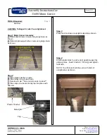
background image

Prepreg

Core

Prepreg

Top Layer

Bottom Layer

PGND

GND

Start-Up of the EVM and Power Sequences

www.ti.com

Figure 4. Evaluation Board Stackup

4-layer board FR4

Material thickness 1.616 ± 10% mm

Surface finish immersion gold

6

Start-Up of the EVM and Power Sequences

The TPS61193 or TPS61193-Q1 EVM is set up for easy start-up:

Connect LEDs to OUT1 - OUT3 of connector J16. (Note: LED current default is 100 mA and maximum
boost voltage default is 37 V. LED outputs that are not used must be grounded via jumpers J11 to
J14.)

Connect input (BATTERY) voltage 12 V to connector J25.

The LEDs turn on immediately because the jumpers on the EVM are set up for PWM input of 100% duty
cycle. For connector and jumper positions, see

Figure 1

and

Figure 8

.

Input (BATTERY) voltage range is 4.5 V to 40 V.

The TPS61193 or TPS61193-Q1 has a dual function VDDIO/EN pin. By default, VDDIO/EN = 3.3 V is
generated automatically on the EVM from battery input voltage via jumpers J1 and J26. VDDIO/EN acts
as enable for the device as well as supply/reference voltage for IO logic. Device starts when V

IN

voltage is

present and above the V

IN

UVLO voltage level (4 V), and the VDDIO/EN voltage is set above threshold

voltage (1.2 V).

By default, boost switching frequency is 400 kHz (jumper J4 connecting R3 = 160 k

Ω

to FSET) and boost

maximum voltage is 37 V (R12 = 750 k

Ω

and R13 = 130 k

Ω

). See

Section 7.1

and

Section 7.3

for

description on how to change boost settings.

By default, LED current is 100 mA per string (jumper J5 connecting R4= 24 k

Ω

to ISET). See

Section 8.2

for the description on how to change LED current setting.

Alternatively to internal LDO, device circuitry can be powered from external power supply (4.4 V to 5.25 V)
connected to the LDO pin. Internal LDO is disabled in this case.

6.1

PWM Input to Initiate Start-up Sequence

The backlight is started by setting PWM input high. By default, the TPS61193EVM has PWM input set
high (100% duty cycle), which is connected to VDDIO through jumper J2. Alternatively, an external PWM
signal can be connected by removing jumper J2 , shorting pins 3 and 4 on jumper J17, and connecting the
external PWM to connector J18.

6.2

Shutdown Sequence

The backlight is shut down (LEDs turned off) by setting PWM input low or when VDDIO/EN = 0. If
VDDIO/EN is set low, the TPS61193 or TPS61193-Q1 enters low-power mode with the internal LDO
disabled.

8

TPS61193EVM Evaluation Module

SNVU491 – October 2015

Submit Documentation Feedback

Copyright © 2015, Texas Instruments Incorporated

Содержание TPS61193-Q1EVM

Страница 1: ...Using the TPS61193EVM and TPS61193 Q1EVM Evaluation Module User s Guide Literature Number SNVU491 October 2015...

Страница 2: ...1 PWM Input to Initiate Start up Sequence 8 6 2 Shutdown Sequence 8 7 Boost Converter 9 7 1 Switching Frequency 9 7 2 Spread Spectrum and Synchronization 9 7 3 Voltage Control 10 8 LED Current Sinks...

Страница 3: ...age vs R12 10 7 Output Current vs RISET 11 8 Evaluation Board Schematic 12 9 LED Load Board Top Side 14 10 LED Load Board Bottom View 14 11 LED Load Board Schematic Diagram 15 12 Forward Voltage for C...

Страница 4: ...t this interference 1 4 If You Need Assistance Contact your local TI sales representative 2 Introduction The Texas Instruments TPS61193EVM evaluation module EVM helps designers to evaluate the operati...

Страница 5: ...stop start and load dump condition The TPS61193 or TPS61193 Q1 device supports PWM brightness dimming ratio up to 10 000 1 for an input PWM frequency of 200 Hz The device integrates extensive safety...

Страница 6: ...TROL POINTS Hardware Setup www ti com 4 Hardware Setup Figure 1 shows connectors and main components on the TPS61193 or TPS61193 Q1 board Figure 1 Evaluation Board Connectors and Setup 6 TPS61193EVM E...

Страница 7: ...Top Layer Figure 3 Bottom Layer GND See the TPS61193 SNVSAF4 or TPS61193 Q1 datasheet SNVSAC7 for PCB layout guidelines 7 SNVU491 October 2015 TPS61193EVM Evaluation Module Submit Documentation Feedba...

Страница 8: ...and the VDDIO EN voltage is set above threshold voltage 1 2 V By default boost switching frequency is 400 kHz jumper J4 connecting R3 160 k to FSET and boost maximum voltage is 37 V R12 750 k and R13...

Страница 9: ...ency remove jumper J4 short pins 7 and 8 on jumper J17 and connect the external resistor to connector J18 Boost internal parameters are adjusted automatically according to chosen frequency during star...

Страница 10: ...2 V R12 R13 values are in k 2 Figure 6 Converter Maximum Output Voltage vs R12 Maximum voltage should be chosen based on the maximum voltage required for LED strings Recommended maximum voltage is abo...

Страница 11: ...7 Output Current vs RISET 8 3 Brightness Control The TPS61193 or TPS61193 Q1 controls the brightness of the display with conventional PWM Output PWM directly follows the input PWM Input PWM frequency...

Страница 12: ...Schematic www ti com 10 Evaluation Board Schematic Figure 8 Evaluation Board Schematic 12 TPS61193EVM Evaluation Module SNVU491 October 2015 Submit Documentation Feedback Copyright 2015 Texas Instrume...

Страница 13: ...0 Samtec TSW 108 07 G D 2 mil above insulator J16 Header TH 100mil 10x2 Gold plated Samtec TSW 110 07 G D 1 230 mil above insulator J18 Header TH 100mil 10x1 Gold plated Samtec TSW 110 07 G S 1 230 mi...

Страница 14: ...h maximum current 175 mA and maximum forward voltage 3 5 mA at 80 mA 3 3 V typical are used on the board For theTPS61193 or TPS61193 Q1 4 strings are assembled NOTE The LED board is not included with...

Страница 15: ...58 1 2 3 J59 1 2 3 J60 1 2 3 J61 1 2 3 J62 1 2 3 J63 GND 1 2 3 4 J64 D80 D79 D78 D77 D76 D75 D74 D73 1 2 3 J77 1 2 3 J78 1 2 3 J79 1 2 3 J80 1 2 3 J81 1 2 3 J82 1 2 3 J83 1 2 3 J84 GND 1 2 3 4 J85 D10...

Страница 16: ...der 100mi 2x2 Samtec TSW 102 07 G D 7 J85 J106 J127 J2 J21 J23 J42 J44 J63 J65 J84 Header 100mi 3x1 Samtec TSW 103 07 G S 121 J86 J105 J107 J126 J129 J130 Header 100mi 7x1 Samtec TSW 107 07 G S 1 D1 D...

Страница 17: ...ing the warranty period to the address designated by TI and that are determined by TI not to conform to such warranty If TI elects to repair or replace such EVM TI shall have a reasonable time to repa...

Страница 18: ...transmitter has been approved by Industry Canada to operate with the antenna types listed in the user guide with the maximum permissible gain and required antenna impedance for each antenna type indic...

Страница 19: ...ified allowable ranges some circuit components may have elevated case temperatures These components include but are not limited to linear regulators switching transistors pass transistors current sens...

Страница 20: ...REMOVAL OR REINSTALLATION ANCILLARY COSTS TO THE PROCUREMENT OF SUBSTITUTE GOODS OR SERVICES RETESTING OUTSIDE COMPUTER TIME LABOR COSTS LOSS OF GOODWILL LOSS OF PROFITS LOSS OF SAVINGS LOSS OF USE L...

Страница 21: ...sponsible for compliance with all legal regulatory and safety related requirements concerning its products and any use of TI components in its applications notwithstanding any applications related inf...

Отзывы: