background image

Table 4-1. The Functions of Each Test Points (continued)

TEST POINTS NAME

DESCRIPTION

TP13

LOOPA

Input A for loop injection

4.5 Jumper Configuration: Enable Selection

The controller can be enabled and disabled by J3.

Default setting: No Jumper shorts on J3 to Enable the controller.

Table 4-2. Enable Selection

JUMPER POSITION

ENABLE SELECTION

Jumper shorts on J3

Disable the controller

No jumper shorts on J3

Enable the controller

5 EVM Configuration Using the Fusion GUI

In order to configure the TPS53819A controller on the EVM from its default values, it is required to use the 
TI Fusion Digital Power Designer software. It is necessary to have input voltage applied to the EVM prior to 
launching the software so the TPS53819A can respond to the GUI and the GUI can recognize the TPS53819A. 
At least 4.25 V must be applied to the V

DD

 pin to overcome the default UVLO setting.

5.1 Configuration Procedure

1. Adjust the input supply to provide at least 4.25 V.
2. Apply the input voltage to the EVM. Refer to 

Figure 4-3

 for connections and test setup.

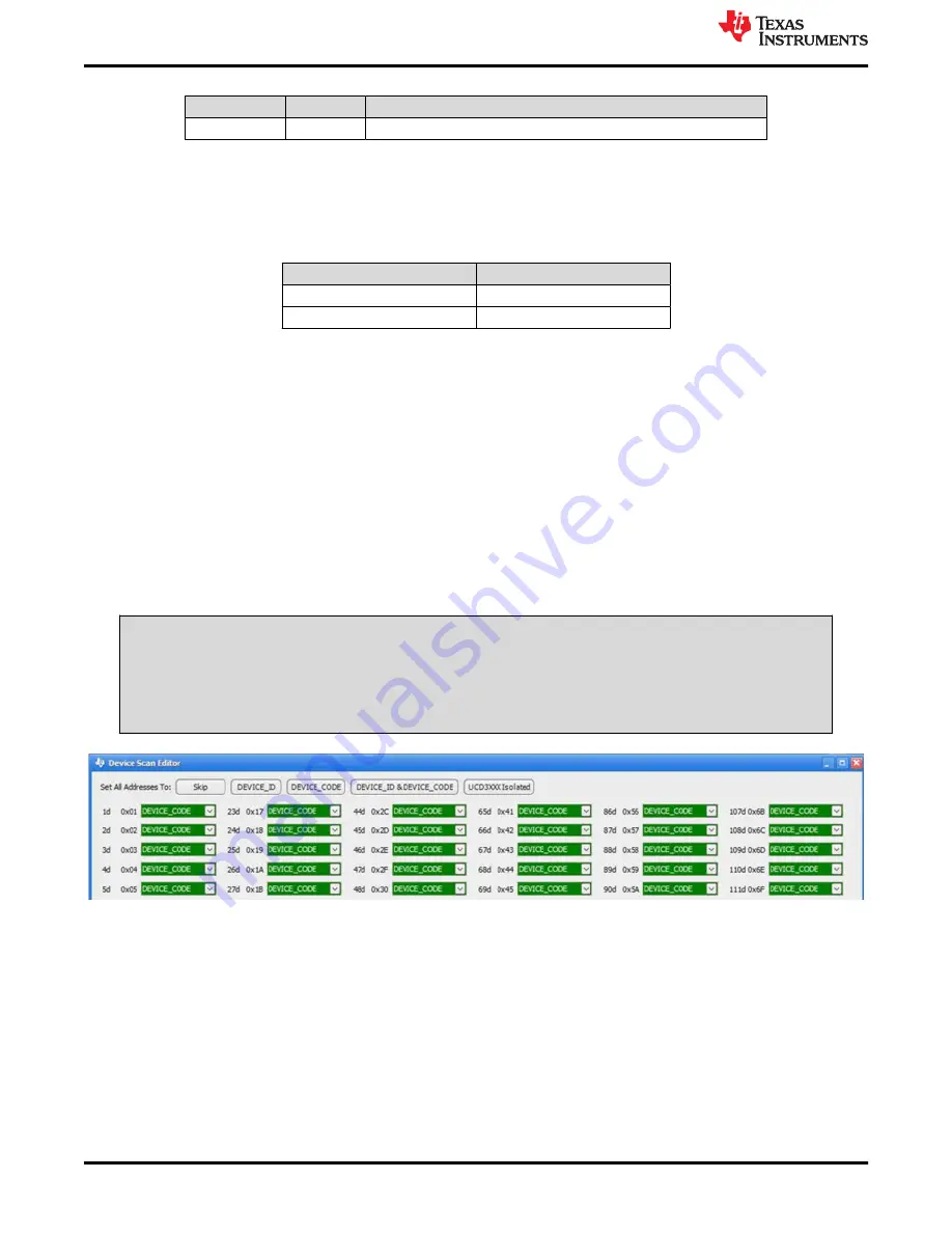
3. Launch the Fusion GUI software. If prompted, select GUI scan mode to 

DEVICE_CODE

 only. Refer to 

Figure 5-1

 for changing device scanning options. The software will recognize the TPS53819A device on the 

EVM and load the GUI.

4. Configure the EVM operating parameters as needed.

CAUTION

Some parameters can be configured, such as switching frequency, to values that can result in erratic 
or unexpected behavior on this EVM. Consult the 

TPS53819A 3-V to 28-V Input, 40-A, Eco-Mode™, 

D-CAP2™ Synchrons Buck Controller Data Sheet

 for guidance in configuration of parameters and 

impact on component selection.

Figure 5-1. Selection of Device Scan Options

5.2 Default Fusion GUI Screenshots and Description

Figure 5-2

 is a screenshot of the 

General

 tab of the Fusion GUI with default configuration where the general 

configuration parameters can be set. After modifying a parameter the 

Write to Hardware

 button must be clicked 

to apply it. When power cycling all parameters reset to the values stored in flash. To change the values stored in 
flash, click the 

Store RAM to Flash

 button. 

Figure 5-3

 is a screenshot of the 

All Config

 tab where all accessible 

registers are viewed. 

Figure 5-4

 is a screenshot of the Status screen selected on the bottom-left corner. The 

USB adapter settings are found in the File menu of the Digital Fusion GUI.

Test Setup

www.ti.com

8

TPS53819A Buck Controller Evaluation Module User's Guide

SLVU719B – MAY 2012 – REVISED NOVEMBER 2021

Submit Document Feedback

Copyright © 2021 Texas Instruments Incorporated

Содержание TPS53819A

Страница 1: ...tware 5 4 2 Test Equipment 5 4 3 Recommended Test Setup 6 4 4 List of Test Points 7 4 5 Jumper Configuration Enable Selection 8 5 EVM Configuration Using the Fusion GUI 8 5 1 Configuration Procedure 8...

Страница 2: ...ard 12 VIN 25 A Fan 20 Figure 7 17 TPS53819AEVM 123 Bottom Board 12 VIN 25 A Fan 21 Figure 8 1 TPS53819AEVM 123 Top Layer Assembly Drawing Top View 22 Figure 8 2 TPS53819AEVM 123 Bottom Layer Assembly...

Страница 3: ...put current VIN 8 V IOUT 25 A 4 3 A No load input current VIN 14 V IOUT 0 A with auto skip mode 1 mA OUTPUT CHARACTERISTICS Output voltage VOUT 1 2 V Output load current IOUT 0 25 A Output voltage reg...

Страница 4: ...6 1 2 3 4 J3 1 2 3 4 J1 C7 0 1uF R2 100k R6 4 7 1 2 3 4 5 6 7 8 9 10 11 12 13 14 15 16 17 U1 Lm LM27403 R10 39 2k C10 100uF L1 0 440uH C2 22uF C5 0 1uF Q1 CSD87350Q5D TP1 TP4 TP5 R8 0 TP8 TP7 TP9 TP3...

Страница 5: ...ble of supplying 30 ADC Connect VIN to J4 as shown in Figure 4 2 Multimeters V1 VIN at TP1 VIN to TP4 PGND V2 VOUT at TP7 VOUT to TP9 PGND A1 VIN input current Output Load The output load should be an...

Страница 6: ...ed wire size is 1 AWG 14 per input connection with the total length of wire less than four feet two feet input two feet return J3 to LOAD The minimum recommended wire size is 2 AWG 14 with the total l...

Страница 7: ...and TP9 to measure the output voltage 4 3 3 Other Connections 1 When using a fan ensure air is flowing across the EVM 2 Connect the ribbon cable from the USB interface adapter to J4 4 4 List of Test...

Страница 8: ...ng options The software will recognize the TPS53819A device on the EVM and load the GUI 4 Configure the EVM operating parameters as needed CAUTION Some parameters can be configured such as switching f...

Страница 9: ...e General Tab www ti com EVM Configuration Using the Fusion GUI SLVU719B MAY 2012 REVISED NOVEMBER 2021 Submit Document Feedback TPS53819A Buck Controller Evaluation Module User s Guide 9 Copyright 20...

Страница 10: ...All Config Tab EVM Configuration Using the Fusion GUI www ti com 10 TPS53819A Buck Controller Evaluation Module User s Guide SLVU719B MAY 2012 REVISED NOVEMBER 2021 Submit Document Feedback Copyright...

Страница 11: ...tatus www ti com EVM Configuration Using the Fusion GUI SLVU719B MAY 2012 REVISED NOVEMBER 2021 Submit Document Feedback TPS53819A Buck Controller Evaluation Module User s Guide 11 Copyright 2021 Texa...

Страница 12: ...for loop response analysis 1 Replace R16 with a 10 resistor 2 Set up EVM as described in Section 4 and Figure 4 3 3 Connect isolation transformer to test points marked TP13 and TP11 4 Connect input s...

Страница 13: ...12VIN FCCM 14VIN FCCM G000 Figure 7 1 TPS53819AEVM 123 Efficiency 7 2 Load Regulation 1 2 1 201 1 202 1 203 1 204 1 205 0 5 10 15 20 25 Output Current A Output Voltage Deviation DCM FCCM VIN 12V G000...

Страница 14: ...d 1 10 100 1000 10000 100000 1000000 0 01 0 1 1 10 100 Input Voltage V Switching Frequency Hz 12VIN DCM 12VIN FCCM G000 Figure 7 4 TPS53819AEVM 123 fSW Versus Load Performance Data and Typical Charact...

Страница 15: ...123 Loop Response Gain and Phase 7 6 Transient Response IOUT VOUT AC Figure 7 6 TPS53819AEVM 123 Load Transient 12 VIN 0 A to 15 A Eco mode www ti com Performance Data and Typical Characteristic Curve...

Страница 16: ...AC VOUT AC SW Figure 7 8 TPS53819AEVM 123 Output Ripple 12 VIN 25 A Performance Data and Typical Characteristic Curves www ti com 16 TPS53819A Buck Controller Evaluation Module User s Guide SLVU719B...

Страница 17: ...re 7 10 TPS53819AEVM 123 Switching Node 12 VIN 25 A Load Full Bandwidth www ti com Performance Data and Typical Characteristic Curves SLVU719B MAY 2012 REVISED NOVEMBER 2021 Submit Document Feedback T...

Страница 18: ...REG VOUT PG Figure 7 12 TPS53819AEVM 123 VIN Turn On Waveform 12 VIN 1 Load Performance Data and Typical Characteristic Curves www ti com 18 TPS53819A Buck Controller Evaluation Module User s Guide SL...

Страница 19: ...VREG VOUT PG Figure 7 14 TPS53819AEVM 123 VIN Turn off Waveform 12 VIN 1 Load www ti com Performance Data and Typical Characteristic Curves SLVU719B MAY 2012 REVISED NOVEMBER 2021 Submit Document Feed...

Страница 20: ...ermal Images Hottest point is the CSD87350Q5D Figure 7 16 TPS53819AEVM 123 Top Board 12 VIN 25 A Fan Performance Data and Typical Characteristic Curves www ti com 20 TPS53819A Buck Controller Evaluati...

Страница 21: ...23 Bottom Board 12 VIN 25 A Fan www ti com Performance Data and Typical Characteristic Curves SLVU719B MAY 2012 REVISED NOVEMBER 2021 Submit Document Feedback TPS53819A Buck Controller Evaluation Modu...

Страница 22: ...2 oz copper circuit board Figure 8 1 TPS53819AEVM 123 Top Layer Assembly Drawing Top View Figure 8 2 TPS53819AEVM 123 Bottom Layer Assembly Drawing Bottom View EVM Assembly Drawing and PCB layout www...

Страница 23: ...PS53819AEVM 123 Internal Layer 1 Top View www ti com EVM Assembly Drawing and PCB layout SLVU719B MAY 2012 REVISED NOVEMBER 2021 Submit Document Feedback TPS53819A Buck Controller Evaluation Module Us...

Страница 24: ...6 TPS53819AEVM 123 Internal Layer 4 Top View EVM Assembly Drawing and PCB layout www ti com 24 TPS53819A Buck Controller Evaluation Module User s Guide SLVU719B MAY 2012 REVISED NOVEMBER 2021 Submit D...

Страница 25: ...8 8 TPS53819AEVM 123 Bottom Copper Top View www ti com EVM Assembly Drawing and PCB layout SLVU719B MAY 2012 REVISED NOVEMBER 2021 Submit Document Feedback TPS53819A Buck Controller Evaluation Module...

Страница 26: ...Chip 1 00 k 1 16W 1 Std Std 2 R6 Resistor Chip 4 7 1 16W 1 Std Std 1 R9 Resistor Chip 3 1 4W 1 Std Std 0 R7 R13 Resistor Chip 1 16W 1 Std Std 1 R10 Resistor Chip 39 2 k 1 16W 1 Std Std 5 R5 R8 R11 R12...

Страница 27: ...ther than TI b the nonconformity resulted from User s design specifications or instructions for such EVMs or improper system design or c User has not paid on time Testing and other quality control tec...

Страница 28: ...These limits are designed to provide reasonable protection against harmful interference in a residential installation This equipment generates uses and can radiate radio frequency energy and if not in...

Страница 29: ...instructions set forth by Radio Law of Japan which includes but is not limited to the instructions below with respect to EVMs which for the avoidance of doubt are stated strictly for convenience and s...

Страница 30: ...any interfaces electronic and or mechanical between the EVM and any human body are designed with suitable isolation and means to safely limit accessible leakage currents to minimize the risk of electr...

Страница 31: ...R DAMAGES ARE CLAIMED THE EXISTENCE OF MORE THAN ONE CLAIM SHALL NOT ENLARGE OR EXTEND THIS LIMIT 9 Return Policy Except as otherwise provided TI does not offer any refunds returns or exchanges Furthe...

Страница 32: ...change without notice TI grants you permission to use these resources only for development of an application that uses the TI products described in the resource Other reproduction and display of thes...

Отзывы: