FSR
detection
Frame pulse
FWID
CLKG
FSG
Pulse
Frame
FPER
CLKGDV
CLKSRG
÷
÷
CLKSP
CLKS
McBSP
internal
clock
SCLKME, CLKSM
synchronization
and clock
GSYNC
0,0
0,1
1,0
1,1
CLKRP
CLKR pin
CLKXP
CLKX pin
Preliminary
www.ti.com
Architecture
11.2.1.7 Enable/Disable the Transmit and Receive Processes
The McBSP has the option to stop-resume the transmit/receive process while the module is in
functional mode (out of transmit/receive reset).
When the transmit/receive disable XDISABLE/RDISABLE bit in XCCR_REG/RCCR_REG register is
set, the McBSP will stop the transmit/receive operation at the next frame boundary (frame corruption
avoided).
As soon as the XDISABLE/RDISABLE bit is cleared, the transmit/receive process will resume at the
next frame boundary.
Note that it is not recommended to use this mechanism together with the possibility to interrogate the
transmit/receive buffer status register (XBUFFSTAT/RBUFFSTAT indicating the occupied/available
buffer locations), since this register is a CPU (OCP) clock synchronous register and does not reflect the
exact number of occupied/free locations available on the functional clock domain.
11.2.2 McBSP Sample Rate Generator
The McBSP contains a sample rate generator that can be used to generate an internal data clock
(CLKG) and an internal frame–synchronization signal (FSG). CLKG can be used for bit shifting on the
data receive (McBSP.DR) pin and/or the data transmit (McBSP.DX) pin. FSG can be used to initiate
frame transfers on McBSP.DR and/or McBSP.DX.
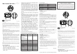
is a conceptual block diagram of the
sample rate generator.
Figure 11-11. Sample Rate Generator Block Diagram
The source clock for the sample rate generator (labeled CLKSRG in the diagram) can be supplied by
either the FCLK functional clock (OCP interface clock), or by an external pin (McBSP.CLKS,
McBSP.CLKX, or McBSP.CLKR). The source is selected with the SCLKME bit of the PCR_REG[7]
register and the CLKSM bit of the SRGR2_REG[13] register.
If a pin is used, the polarity of the incoming signal can be inverted with the appropriate polarity bit
(CLKSP bit of SRGR2_REG[14] register, CLKXP bit of PCR_REG register, or CLKRP bit of
PCR_REG[0] register).
The sample rate generator has a three-stage clock divider that gives CLKG and FSG programmability.
The three stages provide:
•
Clock divide-down. The source clock is divided according to the SRGR1_REG[7:0] register
CLKGDV bits to produce CLKG .
•
Frame period divide-down. CLKG is divided according to the SRGR2_REG[11:0] register FPER bit
field to control the period from the start of a frame–pulse to the start of the next pulse.
1133
SPRUGX9 – 15 April 2011
Multichannel Buffered Serial Port (McBSP)
© 2011, Texas Instruments Incorporated
Содержание TMS320C6A816 Series
Страница 2: ...Preliminary 2 SPRUGX9 15 April 2011 Submit Documentation Feedback 2011 Texas Instruments Incorporated...
Страница 92: ...92 Read This First SPRUGX9 15 April 2011 Submit Documentation Feedback 2011 Texas Instruments Incorporated...
Страница 1122: ...1122 Multichannel Audio Serial Port McASP SPRUGX9 15 April 2011 Submit Documentation Feedback 2011 Texas Instruments Incorporated...
Страница 1562: ...1562 Real Time Clock RTC SPRUGX9 15 April 2011 Submit Documentation Feedback 2011 Texas Instruments Incorporated...
Страница 1658: ...1658 Timers SPRUGX9 15 April 2011 Submit Documentation Feedback 2011 Texas Instruments Incorporated...
Страница 1750: ...1750 UART IrDA CIR Module SPRUGX9 15 April 2011 Submit Documentation Feedback 2011 Texas Instruments Incorporated...
Страница 1984: ...1984 Universal Serial Bus USB SPRUGX9 15 April 2011 Submit Documentation Feedback 2011 Texas Instruments Incorporated...


