background image

2.6.6

Digital Configuration

EVM + PC

www.ti.com

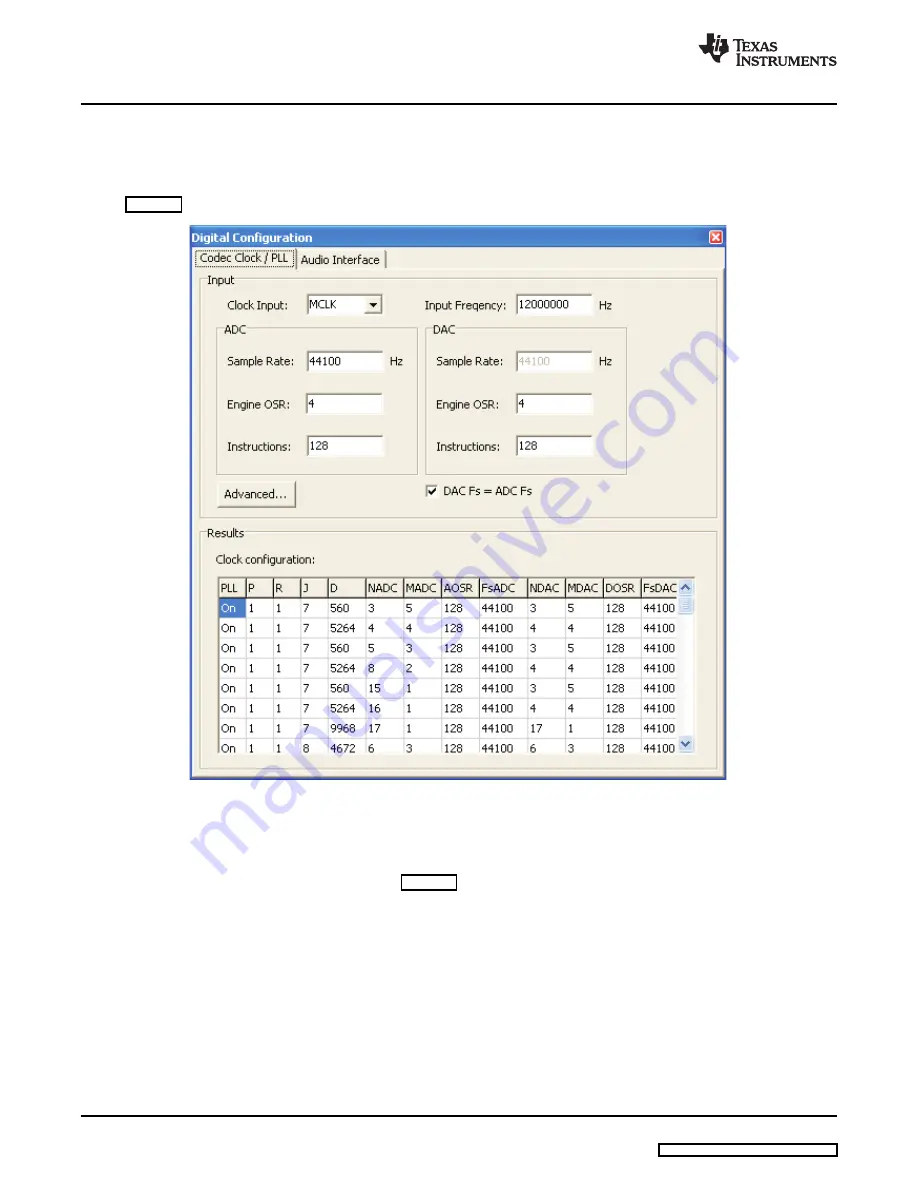
The digital configuration dialog gives access to the codec clock and PLL settings as well as the audio
interface settings.

To open the digital configuration dialog, navigate to the clock and digital signal routing diagram (see

Figure 6

) and click on the “Internal Clock Gen Module” active object.

Figure 7. Digital Configuration: Codec Clock / PLL

The digital configuration dialog contains two tabs, one for the Codec Clock / PLL settings and one for the
Audio Interface settings.

The Codec Clock / PLL settings tab (see

Figure 7

enables simple generation of PLL and clock divider

settings based on the available input frequency and the desired sample rate:

1. Choose the clock input using the Clock Input drop down box.
2. Type the available input frequency in the Input Frequency edit field.
3. Type the desired sample rate in the Sample Rate edit field of the ADC. By default, the DAC sample

rate equals the ADC sample rate. Uncheck DAC Fs = ADC Fs and enter the DAC sample rate for
different sample rates.

4. The Engine OSR and Instructions fields affect the miniDSP. Please contact your TI representative for

further information about the miniDSP.

5. The Results list shows all clock settings that fulfill the chosen parameters. Double click on one of the

results to program the TLV320AIC3111 with the new settings.

Each result has the following columns:

12

TLV320AIC3111 EVM

SLAU285 – July 2009

Submit Documentation Feedback

Содержание TLV320AIC3111 EVM

Страница 1: ...2 1 EVM Preparation 3 2 2 Control Software 3 2 3 Installation 4 2 4 Concepts 4 2 5 Main Window 5 2 6 Dialogs and Active Objects 6 3 EVM Hardware 17 3 1 Connectors and Jumpers 17 3 2 EVM Schematics 20...

Страница 2: ...g and play solution to evaluate the capabilities of the TLV320AIC3111 The USB MODEVM board contains a TAS1020B streaming audio USB controller which enumerates as a USB audio class device When the USB...

Страница 3: ...11 EVM USB MODEVM Note USB MODEVM configuration To control the TLV320AIC3111 from the PC via the USB MODEVM set switch SW2 position 1 3 4 5 6 7 to ON and position 2 and 8 to OFF Connect a headphone to...

Страница 4: ...odules within the TLV320AIC3111 The block diagram consists of active objects that can react to user input for example switches or amplifiers with variable gain that show a volume control on a mouse cl...

Страница 5: ...ecific use case The toolbar contains a control that determines the zoom factor Change the zoom by selecting the desired zoom factor To move the block diagram click on a blank area within the block dia...

Страница 6: ...amplifier active object the function is a volume control Moving the volume control slider changes the volume setting of the amplifier it is also possible to change the volume by clicking onto the numb...

Страница 7: ...detected or if the user selects another use case To show or edit the initialization script choose View Init Script from the main window menu bar Figure 3 Initialization Script Click the Run button to...

Страница 8: ...only text area on the right side of the command dialog displays control data read from the TLV320AIC3111 The Clear button clears the Read Data field The one line text edit field on the left bottom al...

Страница 9: ...mal notation The description column contains a description for each register If the register has no function assigned it is declared Reserved The data columns show the data of each register one byte T...

Страница 10: ...er is in the vicinity showing that it can be selected To change the frequency and gain of a biquad grab and drag its handle It is also possible to change the gain using the slider for each biquad Each...

Страница 11: ...turquoise color To trace the routing of a specific signal follow its color The example in Figure 6 shows that the BCLK signal from the internal clock generation module is routed to the primary I2C BC...

Страница 12: ...ased on the available input frequency and the desired sample rate 1 Choose the clock input using the Clock Input drop down box 2 Type the available input frequency in the Input Frequency edit field 3...

Страница 13: ...cess to the PLL and codec clock dividers It will recalculate the clock results dynamically whenever a parameter is changed The internally generated bit clock signal BCLK can be derived from several so...

Страница 14: ...Right Justified Left Justified For details about the digital audio interface formats see the TLV320AIC3111 data sheet SLAS550 5 4 AUDIO DIGITAL I O INTERFACE The Word Length drop down box defines the...

Страница 15: ...lay in the AGC dialog shows the Amplitude of the ADC output data in decibel with 0dB equal to a full scale signal The target level line can be adjusted using the mouse pointer It will change color to...

Страница 16: ...the DRC transfer function Figure 11 DRC Transfer Function and DRC Dialog The horizontal axis of the DRC transfer function shows the input to the DRC and the vertical axis shows the output of the DRC...

Страница 17: ...3 HP Headphone J14 Headset J15 Headphone Filtered Table 2 Jumpers Jumper Function Positions Default W1 MIC bias select 1 2 3 3V 1 2 3 3V 2 3 EVM W2 W3 On board MIC 1 2 add MIC populated W4 MIC bias to...

Страница 18: ...6 NC P4 7 J4 7 NC P4 8 J4 8 NC P4 9 J4 9 NC P4 10 J4 10 DGND Digital Ground P4 11 J4 11 NC P4 12 J4 12 NC P4 13 J4 13 NC P4 14 J4 14 RESET TAS1020B Reset P4 15 J4 15 NC P4 16 J4 16 NC P4 17 J4 17 NC...

Страница 19: ...DGND Digital Ground P5 19 J5 19 NC P22 20 J5 20 SDA I2C Data Table 5 Power Supply Pin Number Signal P3 1 J3 1 NC P3 2 J3 2 NC P3 3 J3 3 5VA P3 4 J3 4 NC P3 5 J3 5 DGND P3 6 J3 6 AGND P3 7 J3 7 1 8VD...

Страница 20: ...3 2 EVM Schematics EVM Hardware www ti com The schematic diagram for the TLV320AIC3111EVM is provided as a reference TLV320AIC3111 EVM 20 SLAU285 July 2009 Submit Documentation Feedback...

Страница 21: ...C1LP MIC1RP MIC1LP INPUT CONFIGURATION DIFFERENTIAL OUT 2 3 OUT MIC1LP MIC1LM CODEC INPUTS MIC1RP OUT 1 2 1 2 MODE MIC1LM is AC coupled to AVSS ring is connected to MIC1RP Stereo electret microphones...

Страница 22: ...O3 12 GPIO4 14 SCL 16 DGND 18 SDA 20 CNTL 1 CLKX 3 CLKR 5 FSX 7 FSR 9 DX 11 DR 13 INT 15 TOUT 17 GPIO5 19 J5 DAUGHTER SERIAL A0 2 A1 4 A2 6 A3 8 A4 10 A5 12 A6 14 A7 16 REF 18 REF 20 A0 1 A1 3 A2 5 A3...

Страница 23: ...ER TESTPOINTS IOVSS 1 IOVDD 2 DVDD 3 DOUT 4 DIN 5 WCLK 6 BCLK 7 MCLK 8 SDA 9 SCL 10 VOL HED_DET 11 MICBIAS 12 MIC1LP 13 MIC1RP 14 MIC1LM 15 AVSS 16 AVDD 17 DVSS 18 SPLM 19 SLVSS 20 SLVDD 21 SPLP 22 SP...

Страница 24: ...F C34 C35 C36 C37 C38 CAP CER 0 1 F 6 3V X5R 10 0402 C39 4 0 1 F C4 C5 C9 C10 CAP CER 0 1 F 25V X7R 0603 1 0 22 F C11 CAP CER 0 22 F 16V X7R 10 0603 3 0 47 F C5 C7 C8 CAP CER 0 47 F 10V X5R 10 0603 4...

Страница 25: ...lled TP13 TP14 TP15 TP16 TEST POINT PC MINI 040 D WHITE TP17 TP18 TP19 TP20 TP21 TP22 TP23 TP24 TP25 TP26 TP27 TP28 TP29 TP30 TP31 TP32 TP33 TP34 TP35 TP36 6 TP1 TP2 TP3 TP4 TP5 TEST POINT PC MULTI PU...

Страница 26: ...endix A USB MODEVM Schematic www ti com Appendix A The schematic diagram for USB MODEVM Interface Board is provided as a reference SLAU285 July 2009 USB MODEVM Schematic 23 Submit Documentation Feedba...

Страница 27: ...PRODUCTS HIGH PERFORMANCE ANALOG DIVISION SEMICONDUCTOR GROUP FRYE D ZERKETTS I C SPOTTS A 1 1 untitled DOCUMENT CONTROL NO 1234567 MCLK BCLK LRCLK I2SDIN I2SDOUT MISO MOSI SS SCLK RESET INT PWR_DWN P...

Страница 28: ...ER SERIAL 5VD 5VA A0 2 A1 4 A2 6 A3 8 A4 10 A5 12 A6 14 A7 16 REF 18 REF 20 A0 1 A1 3 A2 5 A3 7 AGND 9 AGND 11 AGND 13 VCOM 15 AGND 17 AGND 19 J16 DAUGHTER ANALOG 1 8VD 3 3VD 1 8VD 3 3VD 1 2 3 JMP5 1...

Страница 29: ...220 GREEN USB I2S USB MCK USB SPI USB SPI USB I2S USB MCK 1 8VD RESET C24 0 1uF USB ACTIVE USB RST USB RST 2 4 6 1 3 5 7 8 9 10 11 12 J15 EXTERNAL SPI 2 4 6 1 3 5 7 8 9 10 11 12 J14 EXTERNAL AUDIO DA...

Страница 30: ...0J1306K D1 50V 1A Diode MELF SMD Micro Commercial Components DL4001 D2 Yellow Light Emitting Diode Lumex SML LX0603YW TR D3 D7 Green Light Emitting Diode Lumex SML LX0603GW TR D5 Red Light Emitting Di...

Страница 31: ...2 07 L S JMP5 JMP6 3 position jumper 0 1 spacing Samtec TSW 103 07 L S JMP7 3 position dual row jumper 0 1 spacing Samtec TSW 103 07 L D SW1 SMT half pitch 2 position switch C K Division ITT TDA02H0SK...

Страница 32: ...e C 2 The data packet consists of the following bytes shown in Table C 2 Table C 2 Data Packet Configuration BYTE NUMBER TYPE DESCRIPTION 0 Interface Specifies serial interface and operation The two v...

Страница 33: ...f reg addr 2 0x02 3 0xE0 4 0xAA 5 0x55 In each case the TAS1020 returns in an HID interrupt packet the following 0 interface byte status status REQ_ERROR 0x80 INTF_ERROR 0x40 REQ_DONE 0x20 1 for I2 C...

Страница 34: ...ck as 0 0x51 interface INTF_ERROR 1 0xA0 2 0x02 3 0x05 4 0xAA 5 0x55 If the request is malformed that is the interface byte byte 0 takes on a value which is not as previously described the return pack...

Страница 35: ...1000000 The user can also read back from the GPIO to see the state of the pins Assume the previous example was just written to the port pins Example read the GPIO 0 0x08 read GPIO 1 0x00 this value is...

Страница 36: ...ding The delay time is entered in decimal format A series of byte values follows either a read or write command Each byte value is expressed in hexadecimal and each byte must be separated by a space C...

Страница 37: ...denotes a don t care f 30 01 xxxxxxx0 Any text editor can be used to write these scripts Jedit is an editor that is highly recommended for general usage For more information go to http www jedit org O...

Страница 38: ...ce TI is not responsible or liable for any such statements TI products are not authorized for use in safety critical applications such as life support where a failure of the TI product would reasonabl...

Страница 39: ...Mouser Electronics Authorized Distributor Click to View Pricing Inventory Delivery Lifecycle Information Texas Instruments TLV320AIC3111EVM K...

Отзывы: