


provides the bill of materials for a typical application using the CC2652PSIP module in
.
For full operation reference design, see the
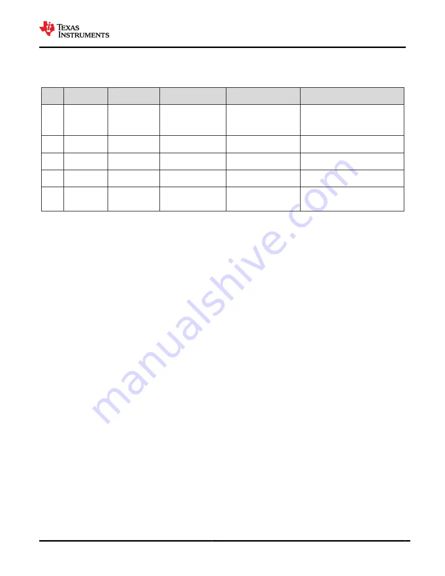
Table 10-1. Bill of Materials
QTY
PART
REFERENCE
VALUE
MANUFACTURER
PART NUMBER
DESCRIPTION
1
ANT1
2.4 GHz Ant
Texas Instruments
N/A
Refer to
for details of the
antenna implementation and PCB
requirements.
1
C1
0.1 µF
Murata
GRT033C81E104KE01D
Capacitor, ceramic, 0.1 µF, 25 V,
±10%, X6S, 0201
1
C2
15 pF
Murata
GRM0332C1H150JA01D
Capacitor, ceramic, 1 pF, 50 V, ±5%,
C0G/NP0, 0201
1
P1
U.FL
Hirose
U.FL-R-SMT-1(01)
U.FL (UMCC) connector receptacle,
male pin 50 Ω, surface mount solder
1
U49
CC2652PSIP
Texas Instruments
CC2652PSIPMOT
SimpleLink™ multiprotocol 2.4-GHz
wireless MCU with integrated power
amplifier
10.2 Device Connection and Layout Fundamentals
10.2.1 Reset
In order to meet the module power-on-reset requirements, an external 0.1 µF capacitor is required on the
nRESET pin during power ON. In addition, VDDS (Pin 46) and VDDS_PU (Pin 47) should be connected
together. If the reset signal is not based upon a power-on-reset and is derived from an external MCU, then the
external capacitor will not be needed and VDDS_PU (Pin 47) should be No Connect (NC). Please refer to
for the recommended circuit implementation and
for the recommended 0.1 µF capacitor.
10.2.2 Unused Pins
All unused pins can be left unconnected without the concern of having leakage current. Please refer to
10.3 PCB Layout Guidelines
This section details the PCB guidelines to speed up the PCB design using the CC2652PSIP module. The
integrator of the CC2652PSIP modules must comply with the PCB layout recommendations described in
the following subsections to minimize the risk with regulatory certifications for the FCC, IC/ISED, ETSI/CE.
Moreover, TI recommends customers to follow the guidelines described in this section to achieve similar
performance to that obtained with the TI reference design.
10.3.1 General Layout Recommendations
Ensure that the following general layout recommendations are followed:
• Have a solid ground plane and ground vias under the module for stable system and thermal dissipation.
• Do not run signal traces underneath the module on a layer where the module is mounted.
SWRS263A – FEBRUARY 2021 – REVISED JUNE 2022
Copyright © 2022 Texas Instruments Incorporated
51
Product Folder Links: