gpmc-006
1 GBytes
512 MBytes
256 MBytes
128 MBytes
64 MBytes
32 MBytes
16 MBytes
A29 A28 A27 A26 A25 A24 A23
…
…
A0
Base address
A29 A28 A27 A26 A25 A24
(16 MBytes minimum granularity)
Mask field
A27 A26 A25 A24
(chip-selects decoding allowing max CS size=256MBytes)
CS size
Mask field
256 MBytes
0
0
0
0
128 MBytes
1
0
0
0
64 MBytes
1
1
0
0
32 MBytes
1
1
1
0
* Mask value like 0010 or 1001 must be avoided
16 MBytes
1
1
1
1
it will create holes in the chip-select address space
Public Version
www.ti.com
General-Purpose Memory Controller
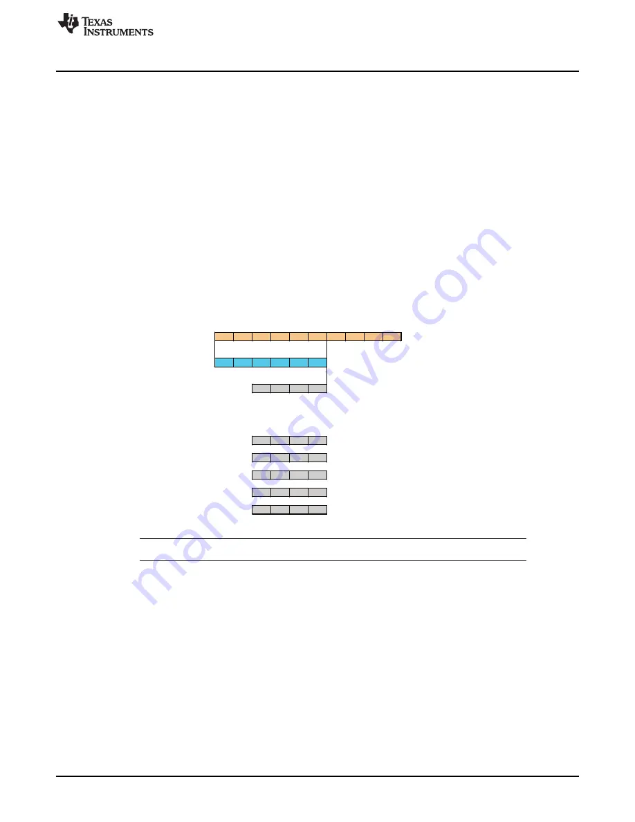
Each chip-select has a 6-bit base address encoding and a 4-bit decoding mask, which must be
programmed according to the following rules:
•
The programmed chip-select region base address must be aligned on the chip-select region size
address boundary and is limited to a power-of-2 address value. During access decoding, the register
base address value is used for address comparison with the address-bit line mapping as described in
(with A0 as the device system byte-address line). Base address is programmed through
the
[5:0] BASEADDRESS bit field
•
The register mask is used to exclude some address lines from the decoding. A register mask bit field
set to 0 suppresses the associated address line from the address comparison (incoming address bit
line is don't care). The register mask value must be limited to the subsequent value, based on the
desired chip-select region size. Any other value has an undefined result. When multiple chip-select
regions with overlapping addresses are enabled concurrently, access to these chip-select regions is
cancelled and a GPMC access error is posted. The mask field is programmed through the
[11:8] MASKADDRESS bit field.
Figure 10-6. Chip-Select Address Mapping and Decoding Mask
NOTE:
GPMC can address up to 256MB on cs0 and cs1, support 128MB on cs2 to cs7
Chip-select configuration (base and mask address or any protocol and timing settings) must be performed
while the associated chip-select is disabled through the GPMC.
[6] CSVALID bit (where
i stands for the GPMC chip-select value, i = 0 to 7). In addition, a chip-select configuration can be disabled
only if there is no ongoing access to that chip-select. This requires activity monitoring of the prefetch or
write-posting engine if the engine is active on the chip-select. Also, the write buffer state must be
monitored to wait for any posted write completion to the chip-select.
Conversely, before trying to access a chip-select, software must ensure that the chip-select is enabled. To
account for prefetch engine effects, after the chip-select-enable instruction, an NOP instruction (equivalent
to 64 bits) must be executed before the chip-select is accessed.
Any access attempted to a nonvalid GPMC address region (CSVALID disabled or address decoding
outside a valid chip-select region) is not propagated to the external interface and a GPMC access error is
posted. In case of chip-selects overlapping, an error is generated and no access will occur on either
chip-select.
Chip-select 0 is the only chip-select region enabled after either a power-up or a GPMC reset.
2125
SWPU177N – December 2009 – Revised November 2010
Memory Subsystem
Copyright © 2009–2010, Texas Instruments Incorporated
Содержание OMAP36 Series
Страница 174: ...174 List of Tables SWPU177N December 2009 Revised November 2010 Copyright 2009 2010 Texas Instruments Incorporated ...
Страница 692: ...692 MPU Subsystem SWPU177N December 2009 Revised November 2010 Copyright 2009 2010 Texas Instruments Incorporated ...
Страница 1084: ...1084 IVA2 2 Subsystem SWPU177N December 2009 Revised November 2010 Copyright 2009 2010 Texas Instruments Incorporated ...
Страница 1990: ...1990 2D 3D Graphics Accelerator SWPU177N December 2009 Revised November 2010 Copyright 2009 2010 Texas Instruments Incorporated ...
Страница 2334: ...2334 Memory Subsystem SWPU177N December 2009 Revised November 2010 Copyright 2009 2010 Texas Instruments Incorporated ...
Страница 2700: ...2700 Memory Management Units SWPU177N December 2009 Revised November 2010 Copyright 2009 2010 Texas Instruments Incorporated ...
Страница 2868: ...2868 HDQ 1 Wire SWPU177N December 2009 Revised November 2010 Copyright 2009 2010 Texas Instruments Incorporated ...
Страница 2974: ...2974 UART IrDA CIR SWPU177N December 2009 Revised November 2010 Copyright 2009 2010 Texas Instruments Incorporated ...
Страница 3054: ...3054 Multichannel SPI SWPU177N December 2009 Revised November 2010 Copyright 2009 2010 Texas Instruments Incorporated ...
Страница 3462: ...3462 MMC SD SDIO Card Interface SWPU177N December 2009 Revised November 2010 Copyright 2009 2010 Texas Instruments Incorporated ...
Страница 3508: ...3508 General Purpose Interface SWPU177N December 2009 Revised November 2010 Copyright 2009 2010 Texas Instruments Incorporated ...
Страница 3584: ...3584 Initialization SWPU177N December 2009 Revised November 2010 Copyright 2009 2010 Texas Instruments Incorporated ...
Страница 3648: ...3648 Debug and Emulation SWPU177N December 2009 Revised November 2010 Copyright 2009 2010 Texas Instruments Incorporated ...


