background image

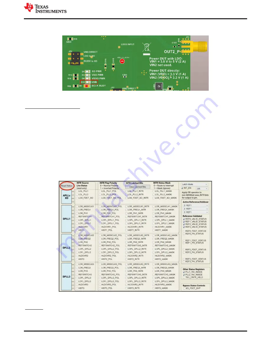
clicking the 

Identify

 button, the LED will flash quickly at about 0.5 seconds on, 0.5 seconds off, for 

about 5 seconds.

Figure 2-1. USB LED

Program the LMK5B33414

1. Toggle the switch S5 (PDN/RESET).
2. Program all the registers:

a. Press the 

Write All Regs

 button in the toolbar.

b. Select 

USB Communications

 in the menu bar, then select 

Write All Registers

, or press Ctrl + L.

3. Check the current consumption. Current consumption should be approximately 1.3 A.
4. Check LMK5B33414 Status as shown in 

Figure 2-2

.

a. Go to the 

Status

 page of the GUI.

b. Click 

Read Status Bits

.

c. Make sure to clear the latched bits. To clear latched bits:

i.

Press the 

Clear Latched Bits

 button.

ii. Select 

Read Status Bits

.

d. Wait to confirm the change. It may take some time for the DPLL status bits to reflect lock.

Figure 2-2. Read Status Bits

Measure 

Measurements can now be made at the clock outputs.

www.ti.com

EVM Quick Start

SNAU279 – JULY 2022

Submit Document Feedback

LMK5B33414EVM User's Guide

5

Copyright © 2022 Texas Instruments Incorporated

Содержание LMK5B33414EVM

Страница 1: ... Schematic 17 4 4 LMK5B33414 and Input Reference Inputs IN0 to IN1 Schematic 18 4 5 Clock Outputs OUT0 to OUT3 Schematic 19 4 6 Clock Outputs OUT4 to OUT9 Schematic 20 4 7 Clock Outputs OUT10 to OUT13 and Clock Inputs IN2 and IN3 Schematic 21 4 8 XO Schematic 22 4 9 Logic I O Interfaces Schematic 23 4 10 USB2ANY Schematic 24 5 EVM Bill of Materials 25 5 1 Loop Filter and Vibration Nonsensitive Cap...

Страница 2: ...ee running locked or holdover mode of operation The EVM can be configured through the onboard USB microcontroller MCU interface using a PC with TI s TICS Pro software graphical user interface GUI TICS Pro can be used to program the LMK5B33414 registers Features LMK5B33414 What is Included LMK5B33414EVM 3 ft mini USB cable MPN 3021003 03 What is Needed Windows PC with TICS Pro Software GUI Test Equ...

Страница 3: ...2_P IN1_N IN1_P IN0_N IN0_P OUT10_P OUT10_N OUT11_N OUT11_P OUT12_P OUT12_N OUT13_N OUT13_P OUT0_P OUT0_N OUT1_N OUT1_P OUT7_P OUT7_N OUT6_N OUT6_P OUT4_P OUT4_N OUT5_N OUT5_P OUT3_P OUT3_N OUT2_N OUT2_P VIN1 VIN2 Figure 1 1 LMK5B33414EVM Default Setting of Jumpers and DIP Switches www ti com Introduction SNAU279 JULY 2022 Submit Document Feedback LMK5B33414EVM User s Guide 3 Copyright 2022 Texas ...

Страница 4: ...P N 4 Connect the USB cable to the USB port at J41 Software Setup 1 If not already installed install the TICS Pro software from the TI website TICS Pro Software 2 If the MATLAB R2015b 9 0 64 bit Runtime is not already installed download and install the software from the MathWorks website While optional for programming and evaluating the default profile settings Matlab Runtime is necessary for any ...

Страница 5: ...t consumption should be approximately 1 3 A 4 Check LMK5B33414 Status as shown in Figure 2 2 a Go to the Status page of the GUI b Click Read Status Bits c Make sure to clear the latched bits To clear latched bits i Press the Clear Latched Bits button ii Select Read Status Bits d Wait to confirm the change It may take some time for the DPLL status bits to reflect lock Figure 2 2 Read Status Bits Me...

Страница 6: ...ty and allow narrower DPLL loop bandwidths to be used B J8 SMA connector for external XO To use the external XO remove the jumper from JP4 4 J4 5 J6 7 J37 J39 J40 J38 SMA Ports for Clock Inputs IN0_P N IN1_P N IN2_P N and IN3_P N IN0_N is not populated and IN0_P is configured for single ended input IN1 is configured for a DC coupled differential input IN2 and IN3 are configured for an AC coupled d...

Страница 7: ...3_P OUT0_P OUT0_N OUT1_N OUT1_P OUT7_P OUT7_N OUT6_N OUT6_P OUT4_P OUT4_N OUT5_N OUT5_P OUT3_P OUT3_N OUT2_N OUT2_P VIN1 VIN2 5 5 5 4 2 9 1 6 8 3B 7 3A Figure 3 1 Key Components EVM Top Side www ti com EVM Configuration SNAU279 JULY 2022 Submit Document Feedback LMK5B33414EVM User s Guide 7 Copyright 2022 Texas Instruments Incorporated ...

Страница 8: ...or the VDD VDDO and XO In the direct power configuration mode an external 3 3 V supply is provided to VIN1 to power the VDD pins an external 3 3 V supply is provided to VIN2 to power the VDDO pins and an external 3 3 V supply is provided to VIN3 to power the onboard XO Note Not every power connection is used or required to operate the EVM Other power configurations are possible See the power schem...

Страница 9: ...DO2 to VDDO Plane Tie pins 5 6 adjacent to designator to select external VIN2 to VDDO Plane JP3 XO Tie pins 1 2 opposite to designator to select 3 3V from DCDC1 to XO supply Tie pins 3 4 to select 3 3 V from LDO3 to XO supply Tie pins 5 6 adjacent to designator to select external VIN3 to XO supply 3 2 Logic Inputs and Outputs The logic I O pins of the LMK5B33414 support different functions dependi...

Страница 10: ... 10 kΩ pull up S2 MSP430 S3 3 9 kΩ pull down S4 LED lit high I2C ADD S1 pull up S2 pull down Figure 3 4 SPI Mode Jumper Configuration In SPI mode GPIO2 must also be configured as STATUS or INT SPI Readback Data SDO Active High and CMOS to support SPI readback Figure 3 5 GPIO2 Setting for SPI Mode Figure 3 6 Communication Setup Window Changing from I2C to SPI EVM Configuration www ti com 10 LMK5B33...

Страница 11: ... a reference clock for the Fractional N APLLs The XO input determines the output frequency accuracy and stability in free run or holdover modes For synchronization applications like SyncE or IEEE 1588 the XO input would typically be driven by a low frequency TCXO or OCXO that conforms to the frequency accuracy and holdover stability requirements of the application For proper DPLL operation the XO ...

Страница 12: ...ulated with a 48 MHz 3 3 V LVCMOS low jitter TCXO designated as Y1 3 2 mm 2 5 mm which drives the XO input of the LMK5B33414 with the onboard termination and AC coupling See Figure 3 9 All LMK5B33414 EVMs have a TXC 7N48071001 48 MHz TCXO populated on Y1 Y1 can be used to evaluate various frequency configurations 3 5 2 External Clock Input Another option is to feed an external clock to the XO SMA ...

Страница 13: ...or a high frequency cascaded APLL reference Figure 6 2 shows how to configure the APLL reference to be cascaded from another APLL 3 6 Reference Clock Inputs The LMK5B33414 has four DPLL reference clock input pairs IN0_P N IN1_P N IN2_P N and IN3_P N with configurable input priority and input selection modes The inputs have programmable input type termination and biasing options to support any cloc...

Страница 14: ...h output format LMK5B33414 Output Driver Oscilloscope Internal input biasing RB RB Driver LVDS HSDS HCSL RB Ω open open 50 Figure 3 10 Output Termination Recommendations 2 Ensure all enabled outputs that are not connected to any test equipment have a 50 Ω SMA termination Figure 3 11 shows an example of a 50 Ω SMA termination Figure 3 11 50 Ω SMA Termination EVM Configuration www ti com 14 LMK5B334...

Страница 15: ... XO 2 Outputs were configured as HSDS outputs following the methods described in Section 3 9 Figure 3 12 APLL3 312 5 MHz Phase Noise Performance Figure 3 13 APLL3 156 25 MHz Phase Noise Performance Figure 3 14 APLL3 125 MHz Phase Noise Performance Figure 3 15 APLL3 100 MHz Phase Noise Performance www ti com EVM Configuration SNAU279 JULY 2022 Submit Document Feedback LMK5B33414EVM User s Guide 15 ...

Страница 16: ...2 BLE18PS080SN1 0402 25V 2200pF C514 GND 0402 25V 2200pF C504 TP501 VDD_XO_DCDC DNP 10V 10uF C515 GND GND 1 2 L503 BLE18PS080SN1 0402 25V 2200pF C516 35V 47uF C500 10uF C23 23 2k R8 13 3k R9 1 A LDO REG LDO3 for XO rail 10uF C22 LDO3 OUT 3 3V IN 1 IN 2 IN CP 3 CP 4 EN 5 GND CP 6 GND 7 FB 8 SET 9 OUT FB 10 OUT 11 OUT 12 DAP 13 LP38798SD ADJ NOPB U9 10nF C24 LDO3_IN LDO3 47k R203 0 01uF C156 GND 1 2...

Страница 17: ...DDGPIO FB11 10uF C59 0 1uF C58 0 1uF C55 10uF C56 FB10 TP8 VDD_IN0 DNP TP10 VDD_IN1 DNP TP12 VDD_DIG DNP TP14 VDD_APLL1_XO DNP TP16 VDD_APLL2 DNP TP18 VDD_APLL3 DNP VDD_PLANE VDDO_PLANE VCC_XO TP9 VDDO_01 DNP TP11 VDDO_23 DNP TP13 VDDO_4TO7 DNP TP15 VDDO_8TO13 DNP VDDO_1415 0 1uF C42 0 1uF C48 0 1uF C54 0 1uF C60 0 1uF C30 0 1uF C36 0 1uF C33 0 1uF C39 0 1uF C57 0 1uF C45 0 1uF C51 NT1 NT_0603 0 R...

Страница 18: ... 64 GPIO2 10 CAP1_APLL2 22 CAP2_APLL2 21 CAP3_APLL2 20 CAP_DIG 40 IN0_N 35 IN0_P 34 IN1_N 38 IN1_P 39 U1 EXT SMA XO CLK SMA_XO_P XO2_P 0 R41 1 2 3 4 5 J8 142 0701 201 49 9 R42 DNP XO1_P 0 1uF R40 0 1uF C70 0 1uF C71 25V 100nF C67 25V 0 047µF C68 DNP SMA_IN0_P SMA_IN0_N 0 R30 0 R26 0 R31 0 R27 51 R32 51 R28 DNP R_IN0_P R_IN0_N 100 R29 DNP IN0_N IN0_P SMA_IN1_P SMA_IN1_N 0 R37 0 R33 0 R38 0 R34 51 R...

Страница 19: ..._LenMatch1a ClassName OUT_LenMatch1a ClassName OUT_LenMatch1a ClassName OUT_LenMatch1a ClassName OUT_LenMatch1a ClassName OUT_LenMatch1a ClassName OUT_LenMatch1a ClassName OUT_LenMatch1b ClassName OUT_LenMatch1b ClassName OUT_LenMatch1b ClassName OUT_LenMatch1b ClassName OUT_LenMatch1b ClassName OUT_LenMatch1b ClassName OUT_LenMatch1b ClassName OUT_LenMatch1b 0 R6 0 R10 0 R81 0 R84 0 R7 0 R80 0 R8...

Страница 20: ... HCSL Source may be VCO2 or VCO3 OUT9 Supported formats LVDS HSDS and HCSL Source may be VCO2 or VCO3 SMA_O4_P SMA_O4_N ClassName OUT_LenMatch2a ClassName OUT_LenMatch2a ClassName OUT_LenMatch2a ClassName OUT_LenMatch2a ClassName OUT_LenMatch1a ClassName OUT_LenMatch1a ClassName OUT_LenMatch2b ClassName OUT_LenMatch2b ClassName OUT_LenMatch2a ClassName OUT_LenMatch2b ClassName OUT_LenMatch2a Class...

Страница 21: ...ssName OUT_LenMatch1a ClassName OUT_LenMatch1a ClassName OUT_LenMatch1a ClassName OUT_LenMatch1a ClassName OUT_LenMatch1a ClassName OUT_LenMatch1a ClassName OUT_LenMatch2a ClassName OUT_LenMatch2b ClassName OUT_LenMatch2a ClassName OUT_LenMatch2b ClassName OUT_LenMatch2a ClassName OUT_LenMatch2b ClassName OUT_LenMatch2a ClassName OUT_LenMatch2b ClassName OUT_LenMatch1b ClassName OUT_LenMatch1b Cla...

Страница 22: ... 2 NC 5 NC 6 GND 7 Y5 ROX2522S4 DNP VCC_XO_FILT EN_XO EN_XO VCC_XO_FILT VCC_XO_FILT VCC_XO_FILT 33 R49 DNP XO3 33 R47 DNP XO3 33 R48 DNP XO3 33 R46 DNP XO3 TP30 Vc DNP 100pF C86 DNP OE 1 NC 2 GND 3 CLK 4 CLK 5 VDD 6 CDC64XX 2520 U4 DNP 33 R50 DNP XO3 VCC_XO_FILT EN_XO 0 1uF C82 0 1uF C83 DNP 0 1uF C85 DNP 0 1uF C87 DNP 0 1uF C84 DNP ClassName XO_trace ClassName XO_trace ClassName XO_trace ClassNam...

Страница 23: ...470 R74 0 R73 6 3 1 8 2 7 5 4 S4 SW_4SPST Active High LED 2 5 mA LMKGPIO2 U2AGPIO5 SOMI 1 5k R58 1 5k R57 U2A_3V3 SH5 1 5k R60 DNP 1 5k R59 DNP U2A_3V3 U2AGPIO6 U2AGPIO2 U2AGPIO0 U2AGPIO1 U2AGPIO4 U2AGPIO5 U2AGPIO8 U2AGPIO5 SOMI U2AGPIO3 U2AGPIO7 SH6 Red 1 2 D6 SCLK BUSY 470 R54 0 R61 1 2 4 U5A U2A_I2CPU SCLK 1 3 D8 DIODE_BAT54 0 01uF C90 100k R62 VDD_PLANE VDDGPIO 0 1uF C89 3 1 2 Q2 FDV301N GND 3...

Страница 24: ...PM_UCB1CLK PM_UCA1STE 48 DVSS2 49 DVCC2 50 P4 4 PM_UCA1TXD PM_UCA1SIMO 51 P4 5 PM_UCA1RXD PM_UCA1SOMI 52 P4 6 PM_NONE 53 P4 7 PM_NONE 54 P5 6 TB0 0 55 P5 7 TB0 1 56 P7 4 TB0 2 57 P7 5 TB0 3 58 P7 6 TB0 4 59 P7 7 TB0CLK MCLK 60 VSSU 61 PU 0 DP 62 PUR 63 PU 1 DM 64 VBUS 65 VUSB 66 V18 67 AVSS2 68 P5 2 XT2IN 69 P5 3 XT2OUT 70 TEST SBWTCK 71 PJ 0 TDO 72 PJ 1 TDI TCLK 73 PJ 2 TMS 74 PJ 3 TCK 75 RST NMI...

Страница 25: ...7R 0603 C1608X7R1H104K080AA TDK C75 C141 2 0 47uF CAP CERM 0 47 uF 10 V 10 X7R 0603 GRM188R71A474KA61D MuRata C89 C132 C133 C137 C138 C142 C143 C144 8 0 1uF CAP CERM 0 1 uF 16 V 5 X7R 0603 C0603C104J4RACTU Kemet C90 C154 C155 C156 4 0 01uF CAP CERM 0 01 uF 50 V 5 X7R 0603 C0603C103J5RACTU Kemet C98 C100 C101 C102 C103 C104 C105 C106 C107 C108 C109 C110 C111 C112 C113 C114 C115 C116 C117 C118 C119 ...

Страница 26: ...ite On D8 1 30V Diode Schottky 30 V 0 2 A SOT 23 BAT54 7 F Diodes Inc FB1 FB2 FB3 FB4 FB5 FB6 FB7 FB8 FB9 FB10 FB11 11 220 ohm Ferrite Bead 220 ohm 100 MHz 2 5 A 0603 BLM18SG221TN1D MuRata FB12 1 300 ohm Ferrite Bead 300 ohm 100 MHz 0 4 A 1 6x0 8x0 95mm LI0603D301R 10 Laird Signal Integrity Products FB13 1 60 ohm Ferrite Bead 60 ohm 100 MHz 3 5 A 0603 MPZ1608S600ATAH0 TDK FID1 FID2 FID3 FID4 FID5 ...

Страница 27: ...FKEA Vishay Dale R2 R5 R9 3 13 3k RES 13 3 k 1 0 1 W AEC Q200 Grade 0 0603 CRCW060313K3FKEA Vishay Dale R6 R7 R10 R80 R81 R83 R84 R87 R89 R91 R93 R95 R97 R98 R100 R102 R104 R106 R107 R108 R110 R112 R114 R116 R118 R120 R123 R124 R126 R128 R130 R132 32 0 RES 0 5 0 063 W AEC Q200 Grade 0 0402 RK73Z1ETTP KOA Speer R11 R12 R16 R17 R18 R19 R20 R21 R22 R23 R25 R41 R52 R55 R61 R64 R66 R71 R73 R150 R151 R1...

Страница 28: ... R166 3 510 RES 510 5 0 1 W AEC Q200 Grade 0 0603 CRCW0603510RJNEA Vishay Dale R168 R170 R171 R172 R173 R174 6 49 9 RES 49 9 1 0 1 W AEC Q200 Grade 0 0402 ERJ 2RKF49R9X Panasonic R201 R202 R203 3 47k RES 47 k 5 0 1 W AEC Q200 Grade 0 0603 CRCW060347K0JNEA Vishay Dale R206 R208 R209 R210 R211 5 0 RES 0 5 0 1 W 0603 RC0603JR 070RL Yageo R501 1 5 60k RES 5 60 k 0 1 0 1 W 0603 RG1608P 562 B T5 Susumu ...

Страница 29: ...e High PSRR LDO DNT0012B WSON 12 LP38798SD ADJ NOPB Texas Instruments U500 1 3A Low Noise and Low Ripple buck converter RPU0010A VQFN 10 TPS62913RPUT Texas Instruments Y1 1 SMD TCXO 7 0 5 0 48 000000MHz 7N48071001 TXC Y6 1 Crystal 24 000 MHz 20pF SMD ECS 240 20 5PX TR ECS Inc C29 C35 0 10uF CAP CERM 10 uF 10 V 20 X5R 0603 C1608X5R1A106M080AC TDK C68 C73 C76 0 0 047uF CAP CERM 0 047 µF 25 V 5 C0G N...

Страница 30: ...2 R125 R127 R129 R131 R133 R134 R135 R136 R137 R138 R139 R140 R141 R142 R143 R167 R169 R175 R176 R177 R178 R179 R180 R181 R182 R183 R184 R185 R186 R187 R188 R189 R190 R191 R204 R205 0 49 9 RES 49 9 1 0 1 W AEC Q200 Grade 0 0402 ERJ 2RKF49R9X Panasonic R192 R193 0 100 RES 100 1 0 063 W AEC Q200 Grade 0 0402 CRCW0402100RFKED Vishay Dale R207 0 0 RES 0 5 0 1 W 0603 RC0603JR 070RL Yageo TP1 TP4 TP7 TP...

Страница 31: ...sidered for vibration immune loop filter components Table 5 2 Examples of Substitute Capacitors Which are Vibration Immune CAPACITOR VALUE VIBRATION SENSITIVE X7R VIBRATION IMMUNE 3 3 nF C0603C332K5RACTU 0603 GRM1885C1H332JA01D C0G NP0 0603 33 nF C0603C333J3RACTU 0603 C2012C0G1H333J125AA C0G NP0 0805 47 nF 06035C473JAT2A 0603 C0805X473G3GEC7800 C0G NP0 0805 C0805C473J3GACTU C0G NP0 0805 0 1 µF C06...

Страница 32: ...cifying the reference to each PLL and associated settings for PLL phase detector frequency 6 1 2 Step 2 Set up the clock input frequencies and the interface type Cascaded APLLs can also be assigned from this page using the PLL R divider and phase detector preview to the right Figure 6 2 Step 1 and 2 XO Input and Clock Inputs Appendix A TICS Pro LMK5B33414 Software www ti com 32 LMK5B33414EVM User ...

Страница 33: ...e APLL post divider frequencies The corresponding APLL is listed next to the REF4 and REF5 The REF with the highest priority will be fed as the DPLL input Figure 6 3 Step 3 DPLL Clock Input Selection 6 1 4 Step 4 Set the clock output for ZDM The PLL will drive the PLL source mux for the selected output set for ZDM Figure 6 4 Step 4 Zero Delay Mode www ti com Appendix A TICS Pro LMK5B33414 Software...

Страница 34: ...cted VCO Frequency box can also be used to copy the VCO frequency in the list selections to the VCO overrides Press the Assign Selected VCO Settings to Device button to update the VCO frequencies then press the Apply Output Clock Settings to Device button By default the analog PLL frequencies are shown The DPLL calculated frequency from step 6 however will result in exact output frequencies After ...

Страница 35: ...ill read all read only registers which provides more information on other pages including the status fields but can take longer to read back The read status bits just reads the status bits for this page For the DPLL to lock a reference must be validated and selected in the Active Reference Holdover and Reference Validated portions of the window shown in Figure 6 8 As the DPLL locks it is expected ...

Страница 36: ...hich can be selected At this time the tool calculates the divider for FB Config 1 only To use two different feedback dividers the following procedure should be preformed 1 Div 1 settings may be copied into Div 2 settings and selected for use by the DPLL Div Select control 2 The references that require the Div 2 settings should be set to FB Config 2 3 You can run a second calculation re perform a r...

Страница 37: ...igure 6 10 PLL3 Input 6 3 1 Cascaded Configurations Cascaded configurations can be created using the input page where the relevant VCO buffers and dividers will automatically be enabled by inferring the state of source selection registers www ti com Appendix A TICS Pro LMK5B33414 Software SNAU279 JULY 2022 Submit Document Feedback LMK5B33414EVM User s Guide 37 Copyright 2022 Texas Instruments Inco...

Страница 38: ...rammed bitwise and is automatically set when generating a frequency plan The XO_OUT_BUF_EN register in the Input Control section of the User Controls tab is automatically set to enable or disable the XO Output Buffer The PLLx_RDIV_XO_EN is automatically checked unchecked in each APLLx tab depending on whether each APLL is using the XO input Located on Inputs page Figure 6 12 APLL Source Box 6 4 Us...

Страница 39: ...post divider for PLL3 PLL3 supports all outputs of the LMK5B33414 Figure 6 14 PLL2 Post Divider Figure 6 15 PLL3 Dividers www ti com Appendix A TICS Pro LMK5B33414 Software SNAU279 JULY 2022 Submit Document Feedback LMK5B33414EVM User s Guide 39 Copyright 2022 Texas Instruments Incorporated ...

Страница 40: ...anced controls that are normally set during the Run Script calculation Figure 6 16 Primary DPLL Controls Appendix A TICS Pro LMK5B33414 Software www ti com 40 LMK5B33414EVM User s Guide SNAU279 JULY 2022 Submit Document Feedback Copyright 2022 Texas Instruments Incorporated ...

Страница 41: ...uency deviation that will be applied to the DPLL numerator This frequency deviation is shown in the DPLLx_FDEV control To perform the shift you must press the increment or decrement button Figure 6 17 DPLL DCO Controls www ti com Appendix A TICS Pro LMK5B33414 Software SNAU279 JULY 2022 Submit Document Feedback LMK5B33414EVM User s Guide 41 Copyright 2022 Texas Instruments Incorporated ...

Страница 42: ...ues Figure 6 18 Validation Page 6 7 Using the GPIO Page The GPIO page allows users to configure the GPIO0 GPIO1 and GPIO2 pins When using SPI readback on the EVM GPIO2 must be configured as STATUS or INT and SDO output When using the device in I2C mode refer to Section 3 3 Figure 6 19 GPIO Page Appendix A TICS Pro LMK5B33414 Software www ti com 42 LMK5B33414EVM User s Guide SNAU279 JULY 2022 Submi...

Страница 43: ...ts on the right hand side of the screen There are many detailed output pages beneath the Outputs page that show the individual controls for each set of outputs The black box around OUT2 to OUT3 OUT4 to OUT7 and OUT8 to OUT13 signifies that all these outputs should source from the same VCO Figure 6 20 Outputs Page www ti com Appendix A TICS Pro LMK5B33414 Software SNAU279 JULY 2022 Submit Document ...

Страница 44: ...other than TI b the nonconformity resulted from User s design specifications or instructions for such EVMs or improper system design or c User has not paid on time Testing and other quality control techniques are used to the extent TI deems necessary TI does not test all parameters of each EVM User s claims against TI under this Section 2 are void if User fails to notify TI of any apparent defects...

Страница 45: ... These limits are designed to provide reasonable protection against harmful interference in a residential installation This equipment generates uses and can radiate radio frequency energy and if not installed and used in accordance with the instructions may cause harmful interference to radio communications However there is no guarantee that interference will not occur in a particular installation...

Страница 46: ...y for convenience and should be verified by User 1 Use EVMs in a shielded room or any other test facility as defined in the notification 173 issued by Ministry of Internal Affairs and Communications on March 28 2006 based on Sub section 1 1 of Article 6 of the Ministry s Rule for Enforcement of Radio Law of Japan 2 Use EVMs only after User obtains the license of Test Radio Station as provided in R...

Страница 47: ... any interfaces electronic and or mechanical between the EVM and any human body are designed with suitable isolation and means to safely limit accessible leakage currents to minimize the risk of electrical shock hazard User assumes all responsibility and liability for any improper or unsafe handling or use of the EVM by User or its employees affiliates contractors or designees 4 4 User assumes all...

Страница 48: ...OR DAMAGES ARE CLAIMED THE EXISTENCE OF MORE THAN ONE CLAIM SHALL NOT ENLARGE OR EXTEND THIS LIMIT 9 Return Policy Except as otherwise provided TI does not offer any refunds returns or exchanges Furthermore no return of EVM s will be accepted if the package has been opened and no return of the EVM s will be accepted if they are damaged or otherwise not in a resalable condition If User feels it has...

Страница 49: ...o change without notice TI grants you permission to use these resources only for development of an application that uses the TI products described in the resource Other reproduction and display of these resources is prohibited No license is granted to any other TI intellectual property right or to any third party intellectual property right TI disclaims responsibility for and you will fully indemn...

Отзывы: