Table of Contents
1 Features
...................................................................................................................................................................................
2
2 Signal Path and Control Circuitry
.........................................................................................................................................
2
3 Getting Started
........................................................................................................................................................................
2
4 Power-Supply Connections
...................................................................................................................................................
2
5 Enabling and Disabling the Outputs
.....................................................................................................................................
3
6 Output Clock
...........................................................................................................................................................................
3
7 Bill of Materials
.......................................................................................................................................................................
4
7.1 REACH Compliance...........................................................................................................................................................
4
8 Schematic
................................................................................................................................................................................
5
9 Revision History
......................................................................................................................................................................
6
Trademarks
All trademarks are the property of their respective owners.
1 Features
• Easy-to-use evaluation board to fan out up to eight LVCMOS clocks with low phase noise, phase jitter
• Output enable pin configurable through jumper
• Board powered from a single 3.3-V, 2.5-V, 1.8-V supply
• Clock output traces are length matched
2 Signal Path and Control Circuitry
The LMK1C1108EVM supports single-ended inputs up to 250 MHz. For more information about the LMK1C1108,
see the LMK1C1108 product data sheet available for download from the TI Web site (
www.ti.com
).
3 Getting Started
The LMK1C1108EVM has self-explanatory labeling and uses similar naming conventions as the LMK1C1108
product data sheet. In this user’s guide, all words in
boldface
reflect the actual labeling on the EVM.
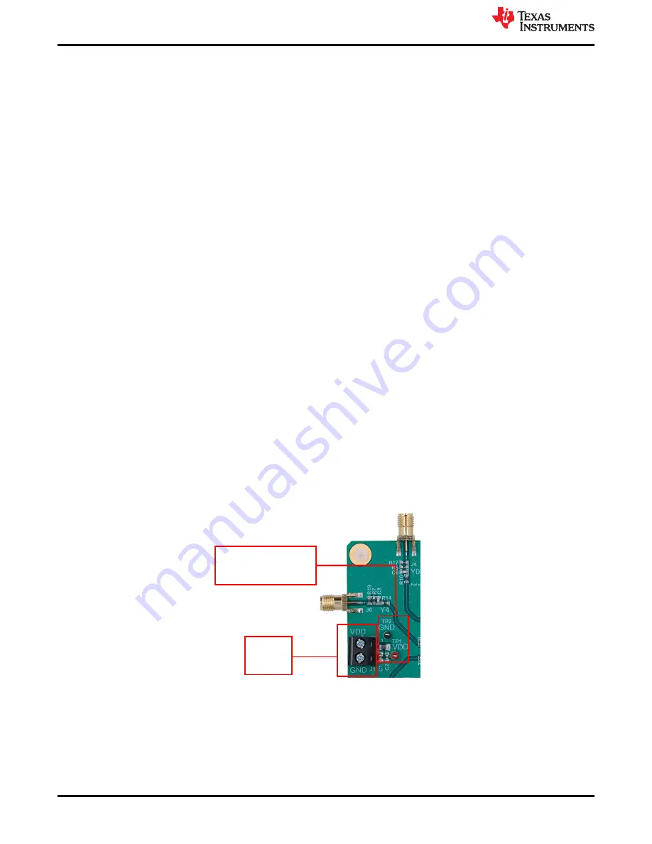
4 Power-Supply Connections
Connect the power-supply source and ground to the terminal block labeled
J1
as shown in
Figure 4-1
.
Alternatively, connect the power-supply source to
TP1
, and connect the ground of the power-supply to
TP2
.
Decoupling capacitors and a ferrite bead isolate the EVM power from the LMK1C1108 device power pins.
TP1 and TP2:
Connect VDD to TP1
Connect GND to TP2
J1
Terminal
Block
Figure 4-1. Power Supply Connection Locations
The LMK1C1108EVM operates from a single 3.3-V, 2.5-V, 1.8-V supply.
Table of Contents
www.ti.com
2
LMK1C1108 Low-Additive, Phase-Noise LVCMOS Clock Buffer Evaluation
Board
SNAU262A – DECEMBER 2020 – REVISED JANUARY 2021
Submit Document Feedback
Copyright © 2021 Texas Instruments Incorporated


