


Connectors
3
SLVUAS3 – June 2016
Copyright © 2016, Texas Instruments Incorporated
DRV8837C Evaluation Module User's Guide
2.1
Test Points
Six test clips are provided for VM, GND, IN1, IN2, DIR, and SPEED REF. Each test point is labeled on the
evaluation module and connects to a same named pin of the DRV8837C device.
lists the
descriptions of these test points.
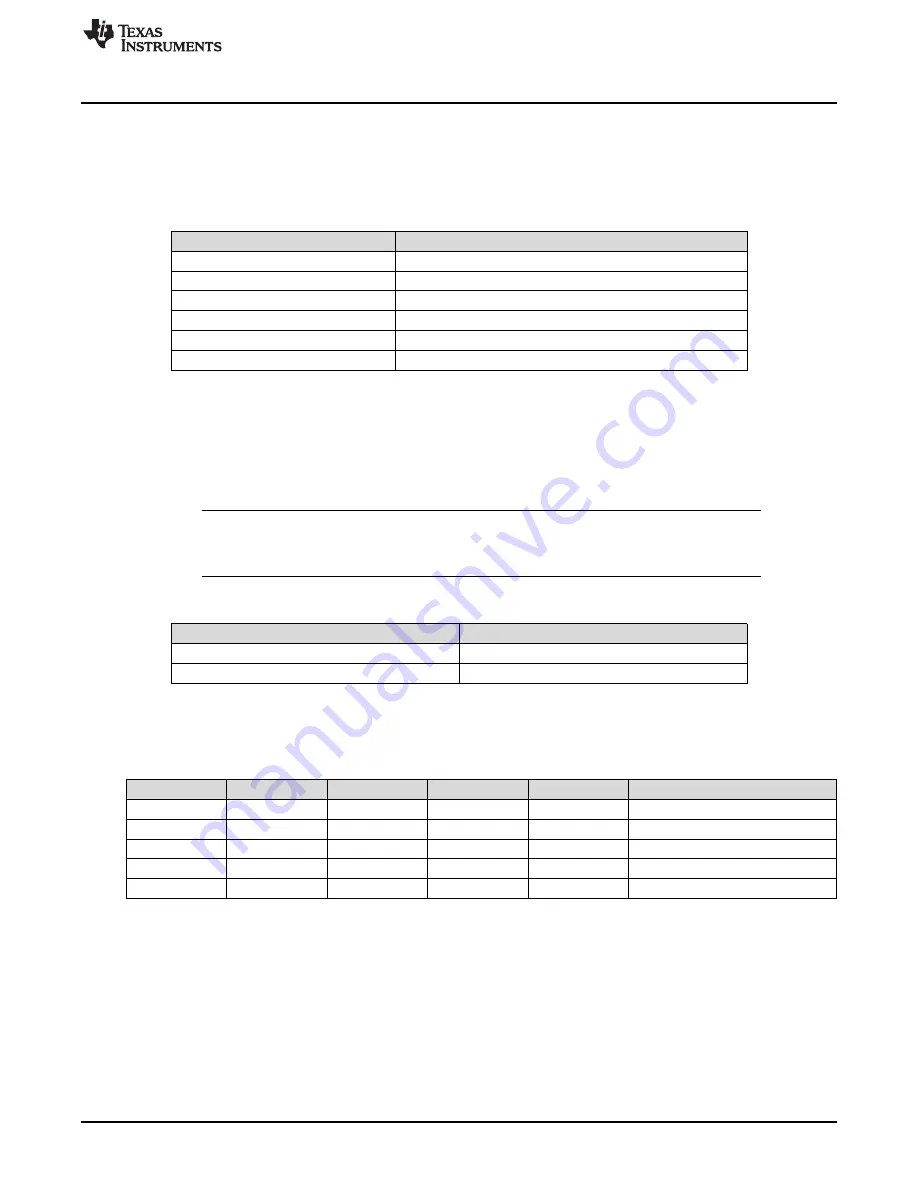
Table 1. Test Point Labels and Descriptions
Test Point Label
Description
VM
Motor voltage rail
GND
Ground plane
IN1
IN1 pin on DRV8837C
IN2
IN2 pin on DRV8837C
DIR
Direction pin on DRV8837C
SPEED REF
ADC pin on MSP430G2131 and 10-k
Ω
potentiometer
2.2
Drive Configuration
The DRV8837C EVM can control the speed and direction of the motor by varying the signals supplied to
the IN1 and IN2 pins on the DRV8837C device. The MSP430G2131 device varies the duty cycle of the
PWM signal supplied to the driver based on the voltage measured between the 10-k
Ω
potentiometer R7.
The direction can be varied using the jumper installed on JP1.
lists the logic for this jumper.
NOTE:
The direction that the motor spins in is dependent on the polarity of the motor lead
connections to the bridge connections. Refer to the data sheet of the motor to determine
which motor terminal should be connected to each driver output.
Table 2. Motor Input Pins and Assigned Headers
Direction Jumper
DIR Pin Voltage
Installed
Forward
Removed
J3, J4
External drive signals can be supplied to the DRV8837C device by removing R1 and R2 from the EVM,
and supplying signals to TP1 and TP2.
lists the drive logic for the DRV8837C device.
Table 3. Motor Input Pin States and Output Conditions
nSLEEP
IN1
IN2
OUT1
OUT2
MOTOR FUNCTION
0
X
X
Z
Z
Coast
1
0
0
Z
Z
Coast
1
0
1
L
H
Reverse
1
1
0
H
L
Forward
1
1
1
L
L
Brake