


2.4
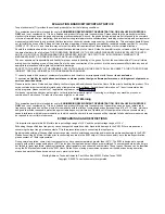
DEM-AS/CDAC Schematics
C024
C020
C016
C012
C002
0.1uF
Vcc1
(NC)
MUTE
V
DD
V
DD
GND
GND
RESET
MDO
MDI
MC
ML
AGND
D_SCLK
CLKO/D_BCK
P_SCLK
DSD_R
P_BCK
P_LRCK
P_DATA
DSD_L
U002
NJM5534
R005
820
C011
2700pF
C005
10uF
/16V
(R003)
C014
10uF/16V
C013
10uF/16V
C010
Jumper
(R004)
V
CC
V
CC
GND
GND
(NC)
(NC)
(NC)
(NC)
V
OUT
L
V
OUT
L+
GND
GND
V
OUT
R
V
OUT
R+
(NC)
AV
CC
AV
CC
+
(NC)
GND
GND
U003
NJM5534
R006
820
C015
2700pF
C018
10uF/16V
C017
10uF
/16V
U004
NJM5534
R009
820
C019
2700pF
(R007)
C022
10uF/16V
C021
10uF
/16V
C016
Jumper
(R008)
U005
NJM5534
R010
820
C023
2700pF
C026
10uF/16V
C025
10uF
/16V
DSDL
DSDR
DBCK
PLRCK/WDCK
PDATA/DFD/PDI
PBCK
SCKI
DGND
V
DD
MS
MDI
MC
MDO
RST
C004
0.1uF
C006
10uF
/16V
R002
10k
C003
10uF
/16V
C001
10uF/16V
U001
DSD1796
(R001)
C009
0.1uF
C008
10uF
/16V
5
2
3
6
4
7
8
5
2
3
6
4
7
8
5
2
3
6
4
7
8
5
2
3
6
4
7
8
22pF
22pF
22pF
22pF
C007
0.1uF
1
2
3
4
5
6
7
8
9
10
11
12
13
14
V
CC
2L
AGND3L
I
OUT
L
IOUTL+
AGND2
V
CC
1
V
COM
L
V
COM
R
AGND1
I
OUT
R
I
OUT
R+
AGND3R
V
CC
2R
I
REF
28
27
26
25
24
23
22
21
20
19
18
17
16
15
Vcc1
www.ti.com
DEM-AS/CDAC Schematics
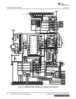
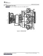
shows the schematic for the sections of the DEM-AS/CDAC.
Figure 2-10. DEM-AS/CDAC
SLEU057A – September 2004 – Revised May 2009
Schematics, PCB Layout, and Bill of Materials
19