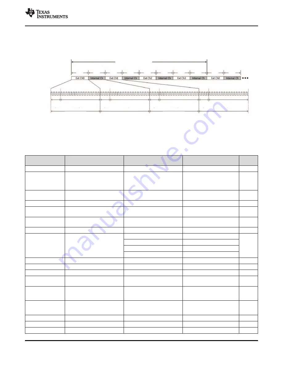
2 µs
2 µs
2 µs
2 µs
2 µs
2 µs
2 µs
2 µs
2 µs
2 µs
Repeats Every 16 µs
ADC CLOCK
= 10 MHz
Sampling
4 cycles
SAR Conversion
16 cycles
Sampling
4 cycles
SAR Conversion
16 cycles
Sampling
4 cycles
SAR Conversion
16 cycles
Sampling
4 cycles
SAR Conversion
16 cycles
EXT CHANNEL 0
INTERNAL CHANNEL
EXT CHANNEL 1
INTERNAL CHANNEL
Internal Ch
59
SWRS224A – FEBRUARY 2019 – REVISED AUGUST 2019
Product Folder Links:
Specifications
Copyright © 2019, Texas Instruments Incorporated
5.18.5.6 ADC
lists the ADC electrical specifications. See
for further information on
using the ADC and for application-specific examples.
Figure 5-15. ADC Clock Timing Diagram
shows the ADC clock timing diagram.
Table 5-22. ADC Electrical Specifications
PARAMETER
DESCRIPTION
TEST CONDITIONS /
ASSUMPTIONS
MIN
TYP
MAX
UNIT
Nbits
Number of bits
12
Bits
INL
Integral nonlinearity
Worst-case deviation from
histogram method over full scale
(not including first and last three
LSB levels)
–2.5
2.5
LSB
DNL
Differential nonlinearity
Worst-case deviation of any step
from ideal
–1
4
LSB
Input range
0
1.4
V
Driving source
impedance
100
Ω
FCLK
Clock rate
Successive approximation input
clock rate
10
MHz
Input capacitance
12
pF
Input impedance
ADC Pin 57
2.15
k
Ω
ADC Pin 58
0.7
ADC Pin 59
2.12
ADC Pin 60
1.17
Number of channels
4
F
sample
Sampling rate of each pin
62.5
KSPS
F_input_max
Maximum input signal frequency
31
kHz
SINAD
Signal-to-noise and distortion
Input frequency DC to 300 Hz
and 1.4 V
pp
sine wave input
55
60
dB
I_active
Active supply current
Average for analog-to-digital
during conversion without
reference current
1.5
mA
I_PD
Power-down supply current for
core supply
Total for analog-to-digital when
not active (this must be the SoC
level test)
1
µA
Absolute offset error
FCLK = 10 MHz
±2
mV
Gain error
±2%
V
ref
ADC reference voltage
1.467
V


