field.
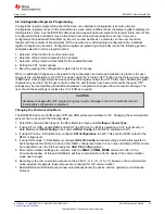
shows the bit field for the Enabled Protections A which is one of the most basic settings that
must typically be changed with the EVM.
Figure 3-6. Data Memory Bit Field Change
Changes to configuration by memory changes take place immediately, however the FETs are enabled using the
Enable_FETs command. Enabling a protection and enabling the protection action on a FET are not sufficient, the
FETs must be enabled with the command.
Calibration data is also located in data memory. Calibration values may be loaded manually or calculated by a
tool.
The
Export
tool in the Data Memory view allows saving the configuration data to a comma-separated-value file
format which can be accessed by a spreadsheet program. Reading data before export with the
Read All
button
will load the data from the part rather than values which may be only in the view. The
Import
tool allows loading
such a saved file into the view so that it can be written to the device. The
Write All
tool writes all values in the
view into registers in the device.
3.6.2 OTP Programming
CAUTION
OTP programming is a permanent change to the device. Be sure all configuration and calibration are
set before programming settings into the device. Casual programming may leave the board
inoperable. Writes to OTP are not incremental, all OTP is written at the same time.
Once the configuration and calibration has been determined and loaded in the registers, it may be programmed
to the BQ76952 OTP memory using the
Program OTP
button at the top of the pane. Note that this is a
permanent programming and is not reversible. There are 2 writes possible, if the device has been programmed
once, a second memory is available. Additional memories are not available. OTP memory is programmed using
the OTP memory view. Programming typically takes about 40 s. To program the OTP memory:
1. OTP write requires 12V at the board stack and room temperature. Calibrate the device if needed.
2. Be sure the desired settings are written to the data memory.
3. Select the Program OTP tool at the top of the Data Memory window. This opens a Program OTP pane.
4. Adjust the board voltage to 12.0 +/- 0.1 V for programming.
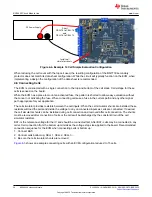
5. Select the Check OTP Programming Possible button. If not successful make the recommended adjustments
if possible. If successful, the display is similar to
6. Select the Program Data Memory to OTP Memory button. If successful, the display is similar to the check.
7. Adjust the board voltage back to normal operating conditions, cycle power, and test as desired.
Battery Management Studio Software
12
BQ76952 Evaluation Module
SLUUC33A – NOVEMBER 2019 – REVISED OCTOBER 2020
Copyright © 2020 Texas Instruments Incorporated


