


Current Path
- +
Sense Path
bq501210EVM-756 Assembly Drawings and Layout
21
SLVUAO6 – June 2016
Copyright © 2016, Texas Instruments Incorporated
bq501210 bqTESLA™ Wireless Power TX EVM
7
bq501210EVM-756 Assembly Drawings and Layout
through
show the design of the bq501210EVM PCB. The EVM layout has been
designed with the intent of easy access to critical notes and, therefore, is not optimized for space. The
EVM has been designed using a 4-layer, 2-oz, copper-clad circuit board, 13.2 cm × 7.24 cm with all
components in a 4.0-cm x 5.0-cm active area on the top side and all active traces to the top and bottom
layers to allow the user to easily view, probe, and evaluate the bq501210 control IC in a practical
application. Moving components to both sides of the PCB or using additional internal layers offers
additional size reduction for space-constrained systems. Gerber files are available for download from the
EVM product folder (
A 4-layer PCB design is recommended to provide a good low-noise ground plane for all circuits. A 2-layer
PCB presents a high risk of poor performance. Grounding between the bq501210 GND pins and filter
capacitor returns for V33A and V33D should be a good low-impedance path.
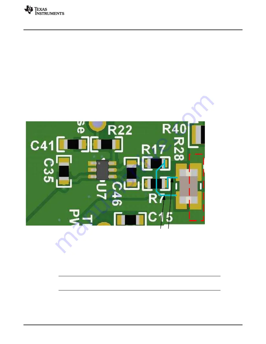
Special note should be taken of R28, the sense resistor in the Current Sense Schematic (
). The
current sense layout is critical in the FOD performance. To get the best performance we use a 4-terminal
resistor which allows the sense pins to go directly to the current monitor eliminating any solder connection
resistance to be eliminated to get the true voltage across the sense resistor.
Figure 14. Sense Resistor Layout
Coil Grounding
– A ground plane area under the coil is recommended to reduce noise coupling into the
receiver. The ground plane for the EVM is slightly larger than the coil footprint and grounded at one point
back to the circuit area.
NOTE:
The clear plastic cover thickness (0.93 in or 2.4 mm) is the z-gap thickness for the
transmitter, which is within the WPC specification limits.