Texas Instruments bq2415 Series Скачать руководство пользователя страница 7

BQ2415x

EVM

DC+

J 1

DC -

BAT+

S

C

L

BAT -

APPLICATION

CIRCUIT

U1

J3

J5

J 4

J2

D1

JMP1

JMP2

JMP3

AUXPWR

CD

S

D

A

D

C

-

D

C

-

S

T

A

T

O

T

G

S

L

R

S

T

JMP5

JMP4

V

I

Power

supply #1

Load

#1

Io

I

I in

USB
Cable

HPA172

Ribbon
Cable

V

www.ti.com

PCB Layout Guideline

2.4.2

Boost Function (For -001, -002, -003, -004, -005, -006, -008 only)

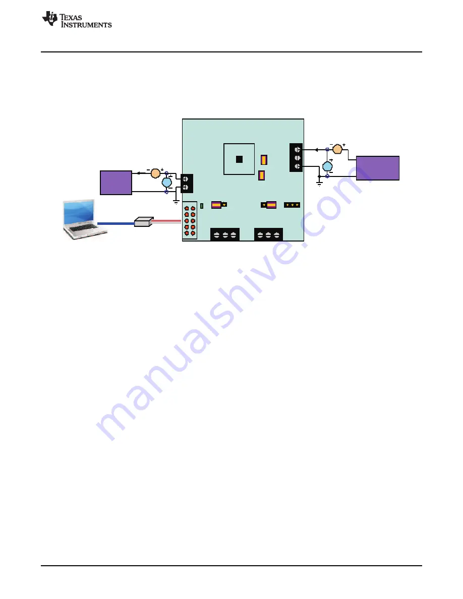
1. Adjust PS#1 output to 3.7V and disable the output. Connect the PS#1 in series with a current meter

(multimeter) to J2 (BAT+, BAT–). Make sure a voltage meter is connected across J2 (BAT+, BAT–).

2. Set the Load #1 current to 200mA ± 20mA but disable the output. Connect the output of the Load #1 in

series with a current meter (multimeter) to J1 (DC+, DC–). Make sure a voltage meter is connected
across J1 (DC+, DC–). The setup is now like

Figure 5

for HPA256.

Figure 5. Test setup for HPA256

3. Turn on PS#1 output
4. Software setup: Change Operation Mode to Boost Mode.

Measure

V(J1(DC+, DC–))=5V ± 0.2V

5. Enable Load #1.

Measure

V(J1(DC+, DC–))=5V ± 0.2V

Measure

Iin = 330mA ± 40mA

Measure

Io = 200mA ± 20mA

3

PCB Layout Guideline

1. To obtain optimal performance, the power input capacitors, connected from input to PGND, should be

placed as close as possible to the IC.

2. The output inductor should be placed close to the IC and the output capacitor connected between the

inductor and PGND of the IC. The intent is to minimize the current path loop area from the SW pin
through the LC filter and back to the PGND pin. To prevent high frequency oscillation problems, proper
layout to minimize high frequency current path loop is critical.

3. The sense resistor should be adjacent to the junction of the inductor and output capacitor. Route the

sense leads connected across the RSNS back to the IC, close to each other (minimize loop area) or
on top of each other on adjacent layers (do not route the sense leads through a high-current path).

4. Place all decoupling capacitor close to their respective IC pin and as close as to PGND (do not place

components such that routing interrupts power stage currents). All small control signals should be
routed away from the high current paths.

5. The PCB should have a ground plane (return) connected directly to the return of all components

through vias (two vias per capacitor for power-stage capacitors, two vias for the IC PGND, one via per
capacitor for small-signal components). A star ground design approach is typically used to keep circuit
block currents isolated (high-power/low-power small-signal) which reduces noise-coupling and
ground-bounce issues. A single ground plane for this design gives good results. With this small layout
and a single ground plane, there is no ground-bounce issue, and having the components segregated
minimizes coupling between signals.

6. The high-current charge paths into VBUS, PMID and from the SW pins must be sized appropriately for

the maximum charge current in order to avoid voltage drops in these traces. The PGND pins should be
connected to the ground plane to return current through the internal low-side FET.

7

SLUU321B – June 2008 – Revised May 2010

bq2415x YFF EVM

Copyright © 2008–2010, Texas Instruments Incorporated

Содержание bq2415 Series

Страница 1: ...q2415x EVM 5 3 The Main Window of the bq2415x Evaluation Software For bq24150 1 2 0A 1A 5 4 The Main Window of the bq24153_6_8 Evaluation Software for bq24153 6 8 6 5 Test setup for HPA256 7 6 Top Layer 10 7 Bottom Layer 10 8 Top Assembly 11 9 Top Silk 11 List of Tables 1 Factory Jumper Settings 4 1 Introduction 1 1 EVM Features Evaluation Module For BQ2415x High Efficiency Fully Integrated NMOS N...

Страница 2: ... positive output connect to CSOUT pin J3 SCL I2 C clock connect to SCL pin J3 SDA I2 C data connect to SDA pin J3 DC AC adapter or USB negative output J4 STAT Status output can be connected to STAT pin by JMP1 set to EXT 2 3 J4 OTG SLRST Connect to OTG SLRST pin J4 DC AC adapter or USB negative output 1 4 Control and Key Parameters Setting Jack Description Factory Setting LED 1 2 Connect STAT pin ...

Страница 3: ... shorted Measure A B Check specified parameters A B If measured values are not within specified limits the unit under test has failed Observe A B Observe if A B occur If they do not occur the unit under test has failed Assembly drawings have location for jumpers test points and individual components 2 2 Equipment 2 2 1 POWER SUPPLIES Power Supply 1 PS 1 a power supply capable of supplying 5 V at 2...

Страница 4: ... sure a voltage meter is connected across J2 BAT BAT Turn on the Load 2 Use the constant voltage mode Set the output voltage to 2 5V E Turn off Load 2 F Connect J5 to HPA172 kit by 10 pin ribbon cable Connect the USB port of the HPA172 kit to the USB port of the computer The connections are shown in Figure 1 Figure 1 Connections of the HPA172 Kit G Installed jumpers per Table 1 Table 1 Factory Jum...

Страница 5: ... Setup for HPA256 bq2415x EVM I Turn on the computer For 001 002 003 004 005 open the bq2415x evaluation software The main window of the software is shown in Figure 3 For 006 007 008 open the bq24153_6_8 evaluation software Select part number bq24153 bq24156 and bq24158 and click GO button The main window of the software is show in Figure 4 Figure 3 The Main Window of the bq2415x Evaluation Softwa...

Страница 6: ... 4 20V For 006 007 008 Make sure Immediate Updates is enabled Check Periodic Resets set Rate to 5 seconds Check Periodic Reads set Rate to 1 second Make sure Operation Mode is Charger Mode Uncheck Charge Current Termination Check STAT Pin Select Charge Current Sense Voltage to Normal Select Battery Regulation Voltage to 4 20V Measure V J2 VBAT VBAT 4 2 100mV Observe D1 is on 3 Enable Load 2 Measur...

Страница 7: ...r layout to minimize high frequency current path loop is critical 3 The sense resistor should be adjacent to the junction of the inductor and output capacitor Route the sense leads connected across the RSNS back to the IC close to each other minimize loop area or on top of each other on adjacent layers do not route the sense leads through a high current path 4 Place all decoupling capacitor close ...

Страница 8: ... 1 1 D2 BAT54C Diode Dual Schottky SOT23 BAT54C Vishay Liteon 200 mA 30 V 1 1 1 1 1 1 1 1 J1 ED1514 2DS Terminal Block 2 pin 0 27 x 0 25 inch ED1514 2DS OST 6 A 3 5mm 3 3 3 3 3 3 3 3 J2 J3 J4 ED1515 3DS Terminal Block 3 pin 0 41 x 0 25 inch ED1515 3DS OST 6 A 3 5mm 1 1 1 1 1 1 1 1 J5 2510 Connector Male 0 338 x 0 788 2510 6002UB 3M 6002UB Straight 2x5 pin 100mil inch spacing 4 Wall 3 3 3 3 3 3 3 3...

Страница 9: ...Polymer Battery 0 0 1 0 0 0 0 0 U1 BQ24152YF IC Battery Charger for WCSP BQ24152YFF TI F Single Cell Li Ion and Li Polymer Battery 0 0 0 1 0 0 0 0 U1 BQ24150AY IC Battery Charger for WCSP BQ24150AYFF TI FF Single Cell Li Ion and Li Polymer Battery 0 0 0 0 1 0 0 0 U1 BQ24151AY IC Battery Charger for WCSP BQ24151AYFF TI FF Single Cell Li Ion and Li Polymer Battery 0 0 0 0 0 1 0 0 U1 BQ24153YF IC Bat...

Страница 10: ...aterials Board Layout and Schematics www ti com 4 2 Board Layout Figure 6 Top Layer Figure 7 Bottom Layer 10 bq2415x YFF EVM SLUU321B June 2008 Revised May 2010 Copyright 2008 2010 Texas Instruments Incorporated ...

Страница 11: ...www ti com Bill of Materials Board Layout and Schematics Figure 8 Top Assembly Figure 9 Top Silk 11 SLUU321B June 2008 Revised May 2010 bq2415x YFF EVM Copyright 2008 2010 Texas Instruments Incorporated ...

Страница 12: ...Bill of Materials Board Layout and Schematics www ti com 4 3 Schematic 12 bq2415x YFF EVM SLUU321B June 2008 Revised May 2010 Copyright 2008 2010 Texas Instruments Incorporated ...

Страница 13: ...oduct This notice contains important safety information about temperatures and voltages For additional information on TI s environmental and or safety programs please contact the TI application engineer or visit www ti com esh No license is granted under any patent right or other intellectual property right of TI covering or relating to any machine process or combination in which such TI products ...

Страница 14: ...ch statements TI products are not authorized for use in safety critical applications such as life support where a failure of the TI product would reasonably be expected to cause severe personal injury or death unless officers of the parties have executed an agreement specifically governing such use Buyers represent that they have all necessary expertise in the safety and regulatory ramifications o...

Отзывы: