TPS65218D0
PMIC
Load Switches 1-3
DDR3 Memory
VTT, VREFCA
VSYS
1.0 V
1.0 V
3.3 V
VDDQ/2
DCDC1
DCDC2
DCDC3
LDO1
Xilinx Zynq 7010
SoC
VCCO_1.5V, VCCO_DDR
VCCPINT
IN_BIAS
400 mA
LSx
VCCINT, VCCBRAM
VDD, VDDQ
IN_DCDCx
IN_LDO
4
1.8 V
DCDC4
VCCAUX, VCCO1.8V,
VCCO_MIO0-1, VCCPAUX,
VCCPLL, VCCADC
1.5 V
(5 V)
LSx_OUT
Regulators
IN_LSx
1.8 A
1.8 A
1.8 A
1.6 A
1.04 A
1.56 A
0.42 A
>0.58 A
VCCO_3.3V
1
1
3
2
3
Re-Programming the EEPROM of the TPS65218D0 Device
17
SLVUBH5 – October 2018
Copyright © 2018, Texas Instruments Incorporated
Software Instructions
(1)
The power-on sequence order is listed for each rail, numbered 1-3.
Figure 16. TPS65218D0 Re-Programming Example Block Diagram
•
When using a new TPS65218D0 sample IC, the EEPROM values will match a bank of one-time
programmable (OTP) values also stored in the device.
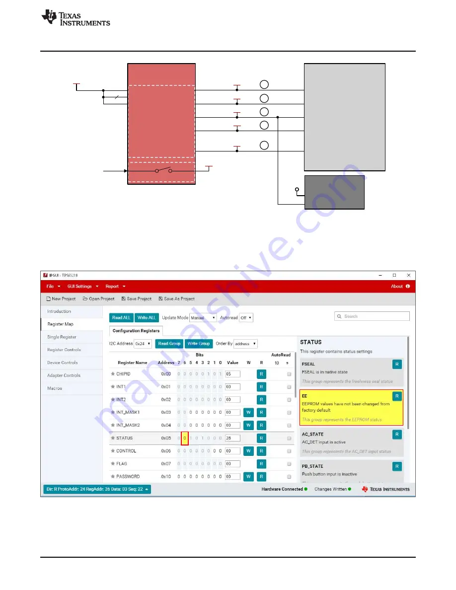
shows that when the EEPROM
values have not yet been re-programmed, bit 6 of the
STATUS
register (0x05) will have a value of 0b.
Figure 17. EEPROM Not Changed (EE Bit = 0b) in Status Register
•
The original value of the
STRICT
bit in the
CONFIG1
register (0x13) is 1b. For this example, the tight
supervisor tolerances are not required, so the
STRICT
bit is changed to 0b, as shown in
.
Similarly, the dynamic voltage scaling of the TPS65218D0 device is not required. As a result, the value
of the
DC12_RST
bit in
CONFIG2
register (0x14) is set to 0b to disable the feature that allows GPIO3


