Texas Instruments AWR1843AOP EVM Скачать руководство пользователя страница 7

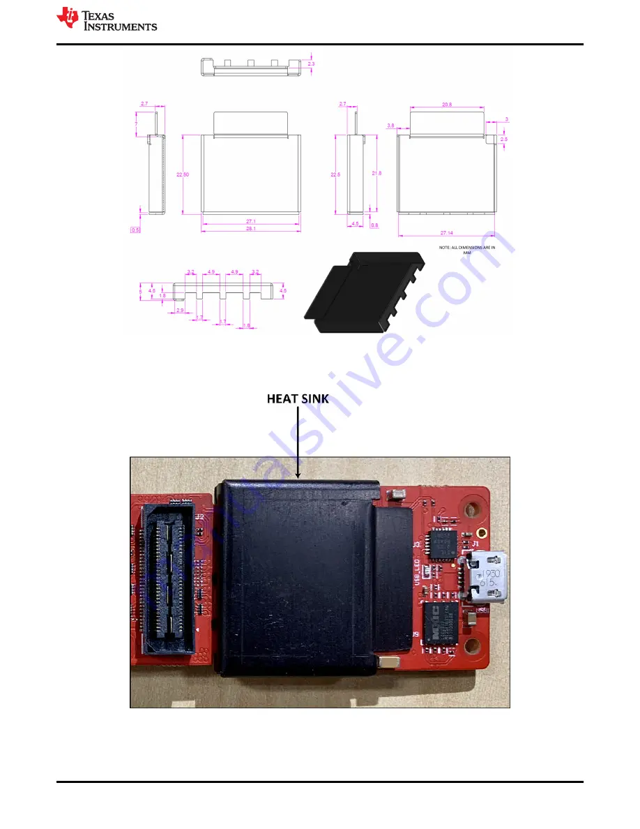
Figure 2-5. Heat Sink CAD Drawing

Application of the heat sink is shown in 

Figure 2-6

.

Figure 2-6. Heat Sink Placement

www.ti.com

Hardware

SPRUIX8 – MARCH 2021

Submit Document Feedback

AWR1843AoP EVM User’s Guide

7

Copyright © 2021 Texas Instruments Incorporated

Содержание AWR1843AOP EVM

Страница 1: ...gures Figure 2 1 AWR1843AOPEVM Top View 4 Figure 2 2 AWR1843AOPEVM Bottom View 5 Figure 2 3 Block Diagram of the AWR1843AOPEVM 5 Figure 2 4 Duty Cycle versus Junction Temperature 6 Figure 2 5 Heat Sin...

Страница 2: ...2 27 Time Domain Plot with Transient Ringing on 1 0 V Supply 25 Figure 2 28 Secondary LC Filter on the AWR1843AOPEVM 26 Figure 3 1 LDO Bypass Enable 27 List of Tables Table 2 1 Switches 11 Table 2 2...

Страница 3: ...AWR1843AOP evaluation board Heat sink Mounting stand Micro USB cable Note A 5 V 2 5 A supply brick with a 2 1 mm barrel jack center positive is not included TI recommends using an external power suppl...

Страница 4: ...ring operation a minimum separation distance of 5 centimeters should be maintained between the user and the EVM Note Refer to the Thermal Design Guide for Antenna on Package mmWave Sensor application...

Страница 5: ...ock Diagram Figure 2 3 shows the functional block diagram The mission board side contains the essential components for the TI radar system PMIC SFLASH SOP configuration Filter TI mmWave Radar chip and...

Страница 6: ...4 shows measurement of junction temperature versus duty cycle taken with and without the heat sink As seen in the plot the EVM can safely operate up to 50 duty cycle with or without the heat sink Alt...

Страница 7: ...wing Application of the heat sink is shown in Figure 2 6 Figure 2 6 Heat Sink Placement www ti com Hardware SPRUIX8 MARCH 2021 Submit Document Feedback AWR1843AoP EVM User s Guide 7 Copyright 2021 Tex...

Страница 8: ...ray Figure 2 8 shows the orientation of the AWR1843AOP relative to the PCB This orientation shows that when the EVM is mounted on the provided mounting stand the antenna is in the elevation orientatio...

Страница 9: ...X2 and TX3 and RX1 RX2 RX3 and RX4 together Note Lambda is computed based on a frequency of 78 5 GHz Figure 2 9 Measured Azimuthal Radiation Pattern for All Tx to Rx Pairs Corner Reflector Placed at 4...

Страница 10: ...All Tx to Rx Pairs Corner Reflector Placed at 4 5 Meters with a 1 75 GHz Bandwidth Chirp Starting at 77 75 GHz Hardware www ti com 10 AWR1843AoP EVM User s Guide SPRUIX8 MARCH 2021 Submit Document Fe...

Страница 11: ...BT LCD S2 2 SPI CS routed to 60 pin connector SPI CS routed to BT LCD S2 3 Bluetooth Enable Bluetooth Disable S2 4 Not Connected Not Connected S3 SOP2 Pulled up SOP2 Pulled down SW2 Reset switch SW3 U...

Страница 12: ...Figure 2 12 Location of LEDs on PCB Hardware www ti com 12 AWR1843AoP EVM User s Guide SPRUIX8 MARCH 2021 Submit Document Feedback Copyright 2021 Texas Instruments Incorporated...

Страница 13: ...VEICBOOST the 5 V supply is provided by the MMWAVEICBOOST board so power over the J5 connector is not required When the breakaway section is removed power should come from the USB connector J1 See mor...

Страница 14: ...ut on this connector UART for flashing the onboard serial flash downloading FW through Radar Studio and getting application data sent through the UART MSS logger UART can be used to get MSS code logs...

Страница 15: ...o Connection 7 SPI_CS 8 No Connection 9 SPI_CLK 10 SPI_HOSTINTR 11 SPI_MOSI 12 SPI_MISO 13 DCA1000_PGOOD 14 No Connection 15 DMM_CLK 16 AR_SYNC_IN 17 DMM_SYNC 18 GND 19 DMM_DP0 20 No Connection 21 DMM...

Страница 16: ...debug signals to the MMWAVEICBOOST The Trace and DMM interface lines are also available through this connector not connected by default Figure 2 16 MMWAVEICBOOST HD Connector J2 Table 2 4 J2 Pin Assi...

Страница 17: ...VDS_0P 47 MCU_CLKOUT 48 LVDS_0N 49 PMIC_CLKOUT_SOP2 50 GND 51 AR_WRMRST 52 AR_NERROR_IN 53 I2C_SDA 54 AR_NERROR_OUT 55 I2C_SCL 56 AR_GPIO_0 57 RS232RX 58 AR_GPIO_1 59 RS232TX 60 AR_GPIO_2 2 7 5 I2C Co...

Страница 18: ...8 BT JTAG Connector J7 Table 2 6 J7 Pin Assignment Pin Number Description 1 Bluetooth UART_RX 2 Bluetooth UART_TX 3 Bluetooth NRESET 4 JTAG_TDI 5 GND 6 JTAG_TDO 7 GND 8 JTAG_TCK 9 3 3V 10 JTAG_TMS Har...

Страница 19: ...FD transceivers TCAN1042HGVDRQ1 These signals can be directly wired to the CAN bus Figure 2 19 CAN Connectors J8 J10 Table 2 7 J8 J10 Pin Assignment Pin Number Description 1 CAN_L 2 GND 3 CAN_H www t...

Страница 20: ...e switch is the ON position SOP 1 and 2 are pulled low when the switch is OFF and high when the switch is ON In MMWAVEICBOOST mode the AWR1843AOPEVM is mounted on the MMWAVEICBOOST and the SOP mode is...

Страница 21: ...reless device through Bluetooth Figure 2 20 shows the setup for SICP2015 Figure 2 21 shows the setup for CC2642R2F 1 Figure 2 20 Switch Configuration for Modular Mode Functional Figure 2 21 Switch Con...

Страница 22: ...on the MMWAVEICBOOST such as the JTAG ADC capture CAN LaunchPad connector and so forth Figure 2 22 AWR1843AOPEVM Mounted on MMWAVEICBOOST Hardware www ti com 22 AWR1843AoP EVM User s Guide SPRUIX8 MAR...

Страница 23: ...ctional 2 9 3 DCA1000 Mode This mode enables raw data capture using the DCA1000 EVM Figure 2 24 AWR1843AOPEVM Mounted on the DCA1000 Note The EVM shown in Figure 2 24 is mounted in the elevation orien...

Страница 24: ...y settling at the start of the chirp the idle time TX start time can be set to a value 10 sec In this configuration the firmware keeps some of the RF blocks ON between the chirps For idle time Tx star...

Страница 25: ...CM21BR71A106KE22L Testing has shown that this filter can be optimized for better transient performance by replacing L12 and L14 with the BLM18KG121TH1D part Further optimizations can be made by replac...

Страница 26: ...Figure 2 28 Secondary LC Filter on the AWR1843AOPEVM Hardware www ti com 26 AWR1843AoP EVM User s Guide SPRUIX8 MARCH 2021 Submit Document Feedback Copyright 2021 Texas Instruments Incorporated...

Страница 27: ...LDO Bypass Requirement The AWR1843AOPEVM utilizes a 1 0 V supply on the RF1 and RF2 power rails To support the third transmitter the VOUT_PA output is connected to the RF2 power rail For best perform...

Страница 28: ...DCA1000EVM Data Capture Card User s Guide MMWAVEICBOOST User s Guide References www ti com 28 AWR1843AoP EVM User s Guide SPRUIX8 MARCH 2021 Submit Document Feedback Copyright 2021 Texas Instruments...

Страница 29: ...are subject to change without notice TI grants you permission to use these resources only for development of an application that uses the TI products described in the resource Other reproduction and...

Отзывы: