


B5
B6
B7
B4
B5
B6
B7
B3
B4
B5
B6
B7
D(R/X)
data delay 2
data delay 1
D(R/X)
data delay 0
D(R/X)
FS(R/X)
CLK(R/X)
Á
Á
Á
Á
ÁÁ
ÁÁ
ÁÁ
ÁÁ
ÁÁ
ÁÁ
ÁÁ
ÁÁ
0-bit period
2-bit period
1-bit period
Element 1
DXR to XSR Copy
RBR to DRR copy
CLKR
FSR
DR
CLKX
FSX
DX
Architecture
1208
SPRUH82C – April 2013 – Revised September 2016
Copyright © 2013–2016, Texas Instruments Incorporated
Multichannel Buffered Serial Port (McBSP)
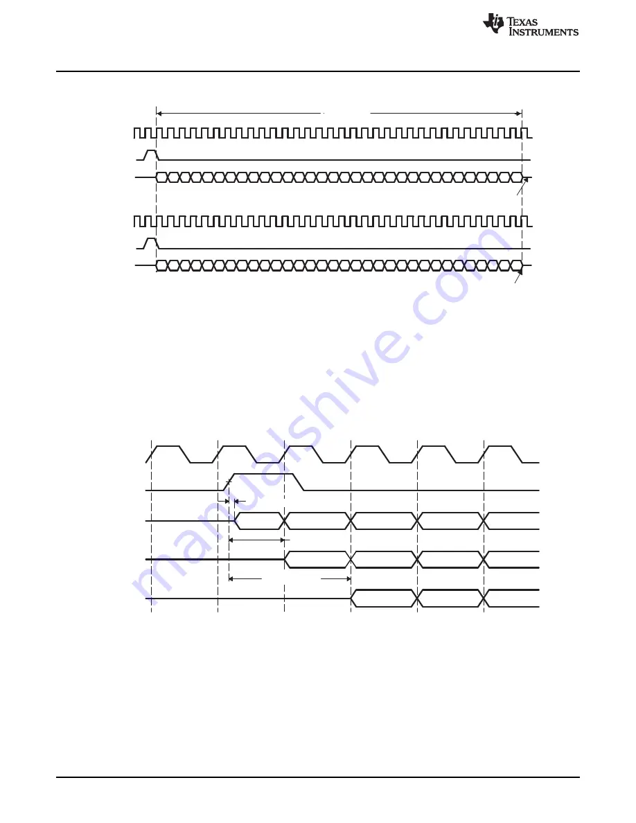
Figure 25-12. Single-Phase Frame of One 32-Bit Element
25.2.5.5.5 Data Delay: RDATDLY and XDATDLY
The start of a frame is defined by the first clock cycle in which frame synchronization is active. The
beginning of actual data reception or transmission with respect to the start of the frame can be delayed if
required. This delay is called data delay. RDATDLY (in RCR) and XDATDLY (in XCR) specify the data
delay for reception and transmission, respectively. The range of programmable data delay is zero to two
bit clocks ((R/X)DATDLY = 00b to10b), as shown in
. Typically, a 1-bit delay is selected
because data often follows a 1-cycle active frame sync pulse.
Figure 25-13. Data Delay
Normally, a frame sync pulse is detected or sampled with respect to an edge of serial clock CLK(R/X).
Thus, on a subsequent cycle (depending on data delay value), data can be received or transmitted.
However, in the case of a 0-bit data delay, the data must be ready for reception and/or transmission on
the same serial clock cycle. For reception, this problem is solved by receive data being sampled on the
first falling edge of CLKR when an active (high) FSR is detected. However, data transmission must begin
on the rising edge of CLKX that generated the frame synchronization. Therefore, the first data bit is
assumed to be in the XSR and DX. The transmitter then asynchronously detects the frame
synchronization, FSX goes active, and it immediately starts driving the first bit to be transmitted on the DX
pin.


