Signal Conditioning
2-2
2.1
Signal Conditioning
The ADS8402/ADS8412EVM comes installed with the unity gain buffer (U2)
wired for single-ended in to differential out configuration. The common-mode
voltage is derived from a REF3040 reference IC and is adjustable using a
potentiometer (R9). The common-mode voltage pin of the THS4503 is set to
2 V on the evaluation module. A single-ended input signal can be applied at
pin connector P1 or via SMA connectors J2 (noninverting input). The buffer
circuit can be reconfigured for a unipolar differential input by installing resistor
R6 and R8 and removing R1. The inverting leg of the differential signal should
be applied to either connector P1 pin 1 or SMA connector J4 (inverting input).
See Table 2 - 1 for the pinout of the analog connector, P1. See Chapter 6 for
the EVM schematic.
Table 2 - 1. Analog Input Connector
Description
Signal Name
Connector.Pin#
Signal Name
Description
Inverting input
( - )
P1.1
P1.2
+
Noninverting input
Reserved
N/A
P1.3
P1.4
N/A
Reserved
Reserved
N/A
P1.5
P1.6
N/A
Reserved
Reserved
N/A
P1.7
P1.8
N/A
Reserved
Pin tied to ground
AGND
P1.9
P.10
N/A
Reserved
Pin tied to ground
AGND
P1.11
P1.12
N/A
Reserved
Reserved
N/A
P1.13
P1.14
N/A
Reserved
Pin tied to ground
AGND
P1.15
P1.16
N/A
Reserved
Pin tied to ground
AGND
P1.17
P1.18
N/A
Reserved
Reserved
N/A
P1.19
P1.20
REF+
External reference input
It is recommended the analog input to any SAR-type converter be buffered.
The amplifier circuit in Figure 2 - 1 is the buffer circuit used on the
ADS8402/ADS8412EVM. This circuit consists of the THS4503, a high-speed
fully differential amplifier configured as a single-ended in to differential out,
unity gain buffer. The circuit shown in Figure 2 - 1 was optimized to achieve the
ac (i.e., SNR, THD, SFDR, etc.) specifications listed in the ADS8402 and
ADS8412 data sheets. The 60-pF and 6800-pF capacitors in the signal path
are polypropylene type, manufactured by the WIMA Corporation.
Polypropylene capacitors cause the least distortion of the input signal.
Содержание ADS8402
Страница 1: ...ADS8402 ADS8412EVM December 2003 Data Acquistion User s Guide SLAU126 ...
Страница 14: ...2 4 ...
Страница 18: ...4 2 ...
Страница 24: ...ADS8402 ADS8412EVM Layout 6 4 6 2 ADS8402 ADS8412EVM Layout Figure 6 1 Top Layer Layer 1 Figure 1 ...
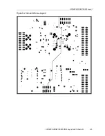
Страница 25: ...ADS8402 ADS8412EVM Layout 6 5 ADS8402 ADS8412EVM BOM Layout and Schematic Figure 6 2 Ground Plane Layer 2 ...
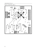
Страница 26: ...ADS8402 ADS8412EVM Layout 6 6 Figure 6 3 Power Plane Layer 3 ...
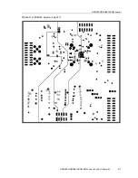
Страница 27: ...ADS8402 ADS8412EVM Layout 6 7 ADS8402 ADS8412EVM BOM Layout and Schematic Figure 6 4 Bottom Layer Layer 4 ...


