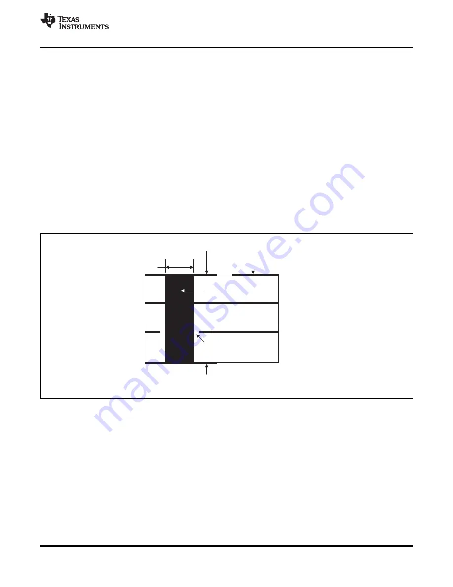
13mils (0.33mm)
Package
Thermal Pad
Component
Traces
Thermal Via
Component (top) Side
Ground Plane
Power Plane
Solder (bottom) Side
Thermal Isolation
(power plane only)
Package
Thermal Pad
(bottom trace)
SBAS367F
–
JUNE 2007
–
REVISED FEBRUARY 2011
PowerPAD PCB Layout Considerations
The via connections to the thermal pad and internal
ground plane should be plated completely around the
shows the recommended layer structure for
hole, as opposed to the typical web or spoke thermal
thermal
management
when
using
a
PowerPad
relief connection. Plating entirely around the thermal
package on a 4-layer PCB design. Note that the
via provides the most efficient thermal connection to
thermal pad is placed on both the top and bottom
the ground plane.
sides of the board. The ground plane is used as the
heatsink, while the power plane is thermally isolated
Additional PowerPAD Package Information
from the thermal vias.
Texas
Instruments
publishes
the
PowerPAD
shows the required thermal pad etch
Thermally Enhanced Package Application Report (TI
pattern for the HTQFP-64 package used for the
literature number
), available for download
ADS1274. Nine 13mil (0.33mm) thermal vias plated
at
that
provides
a
more
detailed
with 1 ounce of copper are placed within the thermal
discussion
of
PowerPAD
design
and
layout
pad area for the purpose of connecting the pad to the
considerations. Before attempting a board layout with
ground plane layer. The ground plane is used as a
the ADS1274, it is recommended that the hardware
heatsink in this application. It is very important that
engineer and/or layout designer be familiar with the
the thermal via diameter be no larger than 13mils in
information contained in this document.
order to avoid solder wicking during the reflow
process. Solder wicking results in thermal voids that
reduce heat dissipation efficiency and hampers heat
flow away from the IC die.
Figure 92. Recommended PCB Structure for a 4-Layer Board
©
2007
–
2011, Texas Instruments Incorporated
41
Product Folder Link(s):


