PC
USB
J15
J5
USB Mini-B
Signal Generator
(Input Source)
Signal
Generator
(CLK Source)
CLK
J9
CHB
J4
CHA
J1
+5V
J5
J12
TSW1400
J3
CHC
J5
CHD
J8
+5V
To A, B, C, D
Channels
BPF
BPF
Synchronized
Sources
Basic Test Procedure
3
Basic Test Procedure
This section outlines the basic test procedure for testing the EVM. There are 2 test platforms which can be
used: (1) TSW1400 with ADC32xx and ADC34xx and (2) TSW14J56 with ADC32Jxx and ADC34Jxx.
3.1
Test Block Diagram with ADC32xx and ADC34xx
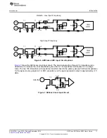
shows the test set-up for evaluation of the ADC3xxxx EVM with the TSW1400 Capture Card. As
seen in this figure, the evaluation setup involves a clock from a high-quality signal generator and a sine
wave for the analog input from a high-quality signal generator. High order, narrow bandpass filters are
usually required on clock and input frequencies to remove phase noise and harmonic content from the
input sine waves. If the two signal generators are not synchronized by an external reference signal to
make the clock and input frequency coherent, then the resulting fast Fourier transform (FFT) will first need
to have a windowing function such as Blackman-Harris/Hamming/Hanning applied to the data.
Figure 13. ADC32xx/ADC34xx and TSW1400 Test Setup Block Diagram
21
SLAU579A – June 2014 – Revised September 2014
ADC3xxx, ADC3xJxx EVM User’s Guide
Copyright © 2014, Texas Instruments Incorporated


