


CLK IN
1:4
0.1
P
F
0.1
P
F
:
:
0.1
P
F
14bit
ADC
Jp
Jn
39nH
39nH
:
:
:
:
0.1
P
F
0.1
P
F
0.1
P
F
0.1
P
F
15
:
15
:
:
:
10pF
10pF
1:1
1:1
V
CM
0
:
0
:
0.1
P
F
0.1
P
F
14bit
ADC
Jp
Jn
:
:
:
:
0.1
P
F
0.1
P
F
0.1
P
F
0.1
P
F
:
:
:
:
56nH
10pF
1:1
1:1
V
CM
10
:
10
:
0.1
P
F
0.1
P
F
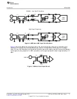
Default
±
Low Input Frequency
High Input Frequency
Introduction
Figure 6. ADC3xxxx ADC Input Circuit options
shows the ADC3xxxx clock input circuit. The clock signal will go through 1:4 impedance ratio
transformer to increase the clock amplitude by two (that is, 1:4 impedance ratio equals to 1:2 voltage
ratio). The two 100-
Ω
resistors will impedance transform back to the primary side as 50-
Ω
load impedance
for the signal source generator. For ADC evaluation, set the signal generator output to approxi10
dBm.
Figure 7. DC34xx Clock Input Circuit
11
SLAU579A – June 2014 – Revised September 2014
ADC3xxx, ADC3xJxx EVM User’s Guide
Copyright © 2014, Texas Instruments Incorporated