Teridian 71M6513 Скачать руководство пользователя страница 1


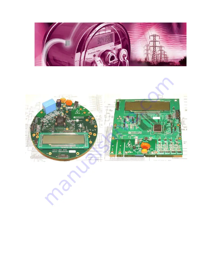
71M6513/71M6513H Demo Board 

USER’S MANUAL 


4/9/2007 10:06 AM 

Revision 5.6 


TERIDIAN Semiconductor Corporation 

6440 Oak Canyon Rd. 

Irvine, CA 92618-5201 

Phone: (714) 508-8800 

 Fax: (714) 508-8878 

http://www.teridian.com/ 

[email protected] 

Downloaded from: 

http://www.datasheetcatalog.com/

Содержание 71M6513

Страница 1: ...AL 4 9 2007 10 06 AM Revision 5 6 TERIDIAN Semiconductor Corporation 6440 Oak Canyon Rd Irvine CA 92618 5201 Phone 714 508 8800 Fax 714 508 8878 http www teridian com meter support teridian com Downlo...

Страница 2: ...ained in the Company s warranty detailed in the TERIDIAN Semiconductor Corporation standard Terms and Conditions The company assumes no responsibility for any errors which may appear in this document...

Страница 3: ...13H Demo Board User s Manual Page 3 of 112 2005 2006 TERIDIAN Semiconductor Corporation Revision 5 6 71M6513 71M6513H 3 Phase Energy Meter IC DEMO BOARD USER S MANUAL Downloaded from http www datashee...

Страница 4: ...eneral Calibration Procedure 28 1 9 2 Calibration Macro File 29 1 9 3 Updating the 6513_demo hex file 29 1 9 4 Updating Calibration Data in Flash Memory without Using the ICE or a Programmer 29 1 9 5...

Страница 5: ...igure 1 1 TERIDIAN D6513T3B2 Demo Board with Debug Board Basic Connections 11 Figure 1 2 Block diagram for the TERIDIAN D6513T3B2 Demonstration Meter with Debug Board 12 Figure 1 3 Block diagram for t...

Страница 6: ...N D6513T3C1 Demo Board Electrical Schematic 2 3 82 Figure 4 6 TERIDIAN D6513T3C1 Demo Board Electrical Schematic 3 3 83 Figure 4 7 TERIDIAN D6513T3D2 Demo Board Electrical Schematic 1 3 84 Figure 4 8...

Страница 7: ...e 1 8 MPU Parameters for Pulse Source Selection 36 Table 1 9 Selectable Pulse Sources 36 Table 1 10 MPU Instantaneous Output Variables 37 Table 1 11 MPU Status Word Bit Assignment 38 Table 1 12 MPU Ac...

Страница 8: ...71M6513 71M6513H Demo Board User s Manual Page 8 of 112 2005 2006 TERIDIAN Semiconductor Corporation Revision 5 6 Downloaded from http www datasheetcatalog com...

Страница 9: ...pre programmed with a Demo Program file name 6513_demo hex in the FLASH memory of the 71M6513 6513H IC This embedded application is developed to exercise all low level function calls to directly mana...

Страница 10: ...their purpose 1 4 DEMO BOARD VERSIONS The following versions of the Demo Board are available Demo Board D6513T3B2 standard Demo Board D6513T3C1 with neutral current detection capability Demo Board D6...

Страница 11: ...ion LED and internal power supply The Debug Board when using a separate power supply is optically isolated from the meter and interfaces to a PC through a 9 pin serial port For serial communication be...

Страница 12: ...PPLY RS 232 INTERFACE DB9 to PC COM Port GND_DBG CYCLE DISPLAY V5_DBG OPTO OPTO FPGA J5 68 Pin Connector to NI PCI 6534 DIO Board OPTO SUPPLY V5_NI CE HEARTBEAT 1Hz MPU HEARTBEAT 5Hz DEBUG BOARD OPTIO...

Страница 13: ...5_DBG OPTO SUPPLY RS 232 INTERFACE DB9 to PC COM Port GND_DBG CYCLE DISPLAY V5_DBG OPTO OPTO FPGA optional J5 68 Pin Connector to NI PCI 6534 DIO Board OPTO SUPPLY V5_NI CE HEARTBEAT 1Hz MPU HEARTBEAT...

Страница 14: ...may be used JP1 and JP2 are plugged in for the straight cable and JP3 JP4 are empty The jumper configuration is reversed for the null modem cable as shown in Table 1 1 Jumpers on Debug Board Cable Co...

Страница 15: ...UP After connecting the DB9 serial port to a PC start the HyperTerminal application and create a session using the following parameters Port Speed 9600 baud Data Bits 8 Parity None Stop Bits 1 Flow Co...

Страница 16: ...ard is a ready to use meter prepared for use with an external current trans former Using the Demo Board involves communicating with the Demo Code via the command line interface CLI The CLI allows all...

Страница 17: ...r parameters Once the Demo Board is connected to a PC or terminal per the instructions given in Section 1 7 2 and 1 7 4 typing will bring up the list of commands shown in Figure 1 6 Figure 1 6 Command...

Страница 18: ...he wait reset command 3 05 only Z Display help on reset Examples Display the command line interpreter help menu C Displays compute engine control help Commands for CE Data Access CE DATA ACCESS Descri...

Страница 19: ...it is set RAM access is limited to the lower 1KB address range Read and write operations will wrap around at higher addresses i e 200 will yield the same result as 0 Commands for DIO RAM Configuration...

Страница 20: ...d issued from the previous command line This is very helpful when examining the value at a certain address over time such as the CE DRAM address for the temperature 0x40 The slash is useful to separat...

Страница 21: ...ring calibration No phase adjustment will be performed Coefficients can be saved to EEPROM using the CLS command Commands controlling the Pulse Counter Function Demo Code Revision 3 05 only CP PULSE C...

Страница 22: ...ation I1 Displays Demo Code version string I1 abcdef Change Demo Code version string I2 Displays Copyright string I3 CE Version string I3 abcdef Change CE Code version string Example I1 Returns Demo C...

Страница 23: ...ndar Date M11 phase V I Angle at Phase degrees M13 1 Main edge count accumulated zero transitions of the input signal M13 2 CE main edge count for the last accumulation interval M14 1 Absolute count f...

Страница 24: ...ode Disables CE ADC CKOUT ECK RTM SSI TMUX VREF and serial port sets MPU clock to 38 4KHz Usage PS Return to normal mode is achieved by resetting the MPU Z command Commands for Controlling the RTC RT...

Страница 25: ...fuse These commands are only accessible for the 71M6513H 0 1 parts When used on a 71M6513 0 5 part the results will be displayed as zero Reset Commands W Z RESET Description Soft Reset and watchdog c...

Страница 26: ...to the dual pin headers on the bottom of the board The Kh value can be derived by reading the values for IMAX and VMAX i e the RMS current and voltage values that correspond to the 250mV maximum inpu...

Страница 27: ...ausing excessive voltages at the 71M6513 inputs Conversely CTs with much higher ratio will tend to decrease the useable signal voltage range at the 71M6513 inputs and may thus decrease resolution 1 8...

Страница 28: ...procedure used parameters calibration constants will result that will have to be applied to the 71M6513 6513H chip in order to make the chip apply the modified gains and phase shifts necessary for ac...

Страница 29: ...no arguments will display the syntax description To merge macro txt and old_6513_demo hex into new_6513_demo hex use the command io_merge old_6513_demo hex macro txt new_6513_demo hex The new hex fil...

Страница 30: ...rating conditions If the phase angle is accurately determined for one current transformer the corresponding phase adjustment coefficient PHADJ_X can be entered for all calibrated units 1 9 6 LOADING T...

Страница 31: ...112 2005 2006 TERIDIAN Semiconductor Corporation Revision 5 6 Figure 1 8 Emulator Window Showing Reset and Erase Buttons see Arrows Figure 1 9 Emulator Window Showing Erased Flash Memory and File Loa...

Страница 32: ...Function E_TCLK Output from 71M6513 6513H Data clock E_RXTX Bi directional Data input output E_RST Bi directional Flash Downloader Reset active low Table 1 5 Flash Programming Interface Signals The ot...

Страница 33: ...ime and enables the user to evaluate the parameters of the metering IC such as accuracy harmonic performance etc It maintains and provides access to basic household functions such as real time clock R...

Страница 34: ...Rh and VAh are not updated and the instantaneous value of IRMS for that element is zeroed LSB 9 4045 10 13 VMAX IMAX Wh Demo Code revision 3 04 The default value is 1536 Demo Code revision 3 05 The de...

Страница 35: ...ement are not zeroed Otherwise the accumulators for Wh VARh and VAh are not updated and the instantaneous value of IRMS for that element is zeroed LSB 9 4045 10 13 IMAX 2 Wh Demo Code revision 3 05 Th...

Страница 36: ...ult for PULSEW_SRC 18 VA2SUM 1 W0SUM 19 WSUM_I Sum of imported real energy 2 W1SUM 20 W0SUM_I Imported real energy on element A 3 W2SUM 21 W1SUM_I Imported real energy on element B 4 VARSUM Default fo...

Страница 37: ...10 4575 4 0x17 0x18 0x19 Irms_A Irms_B Irms_C Irms from element 0 1 2 Nacc In IMAX LSB 8 10 4575 4 8 0x1A 0x1B 0x1C IPhase_A IPhase_B IPhase_C In Vn phase from element n The number of degrees In lags...

Страница 38: ...ed 1 2 SAGB Reserved for sag flag phase B not implemented 1 3 SAGC Reserved for sag flag phase C not implemented 1 4 F0 Reconstructed line signal flag 5 MAXV Overvoltage 1 when overvoltage is detected...

Страница 39: ...d 0x35 VARhe Total VAR hours generated inverse consumed 0x37 VAh Total VA hours 0x39 Wh_A Total Watt hours consumed through element 0 0x3B Whe_A Total Watt hours generated inverse consumed through ele...

Страница 40: ...t measurement is performed by acquiring the signal from a fourth current transformer that is connected to the auxiliary analog input the V3 pin pin 86 The analog data measured on this pin is reference...

Страница 41: ...MUX_RATE 25 100Hz ALT_MUX_RATE 50 51Hz Table 1 14 Neutral Current Accuracy at Various Sampling Frequencies MPU XDATA address 0x027 represents the neutral current RMS value For the standard Demo Code r...

Страница 42: ...71M6513 71M6513H Demo Board User s Manual Page 42 of 112 2005 2006 TERIDIAN Semiconductor Corporation Revision 5 6 Downloaded from http www datasheetcatalog com...

Страница 43: ...in and Phase Errors During the calibration phase we measure errors and then introduce correction factors to nullify their effect With three unknowns to determine we must make at least three measuremen...

Страница 44: ...V E 3a 1 60 cos sin 60 sin cos 60 cos 60 S S XI XV A A E 1 sin 60 tan cos S XI XV S XI XV A A A A Combining 2a and 3a 4 tan 60 tan 1 0 0 60 S E E E 5 60 tan 1 tan 0 0 60 E E E S 6 60 tan 1 tan 0 0 60...

Страница 45: ...g EV E0 E180 E60 and E300 Again set all calibration factors to nominal i e CAL_IA 16384 CAL_VA 16384 PHADJA 0 First calculate AXV from EV 1 1 V XV E A Calculate AXI from E0 and E180 2 1 cos 1 0 cos 0...

Страница 46: ...mean that the calibration system is synchronized to the meter being calibrated Best results are achieved when the first pulse from the meter opens the measurement window of the calibration system This...

Страница 47: ...load current at phase angles 0 and 60 measure the Wh energy and record the errors E0 AND E60 4 Calculate the new calibration factors CAL_IA CAL_VA and PHADJ_A using the formulae presented in section 2...

Страница 48: ...from the characterization data contained in the on chip fuses Tip Step 2 and the energy measurement at 0 of step 3 can be combined into one step 2 2 3 CALIBRATION PROCEDURE FOR ROGOWSKI COIL SENSORS...

Страница 49: ...ws the spreadsheet for five measurements with three phases For CT and shunt calibration data should be entered into the calibration spreadsheets as follows 1 Calibration is performed one phase at a ti...

Страница 50: ...entered in the fields labeled Old CAL_Ix 5 The errors of the energy measurements at 0 60 60 and 180 are entered in the yellow fields labeled Error The spreadsheet will then display phase error the cur...

Страница 51: ...dsheet for Three Measurements 71M6511 71M6513 71M6515 Calibration Worksheet Five Measurements PI 0 019836389 REV 4 2 Ts Date 10 25 2005 AC frequency 50 Hz Author WJH click on yellow field to select fr...

Страница 52: ...hase C old PHADJ 3973 3973 3973 Old CAL_Ix 16384 16384 16384 Error 60 3 712 3 912 5 169 Error 60 3 381 2 915 4 241 Error 0 3 591 3 482 4 751 Error 180 3 72 3 56 4 831 Phase Error 0 0547319 0 1647659 0...

Страница 53: ...ANT 100 Where error observed error at a given voltage V and current I VMAX voltage scaling factor as described in section 1 8 3 IMAX current scaling factor as described in section 1 8 3 LSB QUANT LSB...

Страница 54: ...Software Control Typical Savings Disable the CE CE_EN 0 0 16mA Disable the ADC ADC_DIS 1 1 8mA Disable clock test output CKTEST CKOUTDIS 1 0 6mA Disable emulator clock ECK_DIS 1 0 1mA Set flash read p...

Страница 55: ...dware watchdog timer L1 FERRITE D10 UCLAMP3301D V3P3 1 2 JP1 HDR 1x2 C2 1000pF GND V1 C1 10uF R2 21 5K R1 10K Figure 2 7 Voltage Divider for V1 On the 6513 Demo Boards this feature is implemented with...

Страница 56: ...low to maximize the lifetime of any battery backup device attached to the VBAT pin crystal XOUT XIN 71M651X Figure 2 9 Oscillator Circuit It is not necessary to place an external resistor across the c...

Страница 57: ...gister LCD_BSTEN to 1 starts the on chip boost circuitry that will output an AC frequency on the VDRV pin Using a small coupling capacitor two general purpose diodes and a reservoir capacitor a 5VDC v...

Страница 58: ...t limiting resistor R79 is provided in between the OPT_TX pin of the chip and pin 2 of J12 Figure 2 14 C21 on the D6513T3B2 Demo Boards should be shorted to create a DC path from the collector of the...

Страница 59: ...RX PIN Due to unique circuitry on the RX input its behavior is slightly different from the other digital inputs of the 651X family of metering ICs The Rx pin serial port receive pin of the 71M6513 651...

Страница 60: ...mmended resistor network consisting of R1 17k and R2 33k This network scales the input voltage VIN of 5 5V to 3 6V and an input voltage of 2 5V will be scaled to 1 6V For the low voltage level VIN vol...

Страница 61: ...Board rather receives the voltage output signals fro the CT An optical pickup senses the pulses emitted by the meter and reports them to the calibrator Some calibration systems have electrical pickups...

Страница 62: ...o Code To write a string of text characters to the EEPROM and read it back we apply the following sequence of CLI commands EEC1 Enables the EEPROM EESthis is a test Writes text to the buffer EET80 Wri...

Страница 63: ...etween V1 and V3P3 Conversely removing the jumper at TP10 will enable the hardware watchdog timer 2 5 5 LCD Various tests of the LCD interface can be performed with the Demo Board using the serial com...

Страница 64: ...e the frequency at which SEG and COM pins change states fw CKADC 128 38 400 00 fw 2 9 01 fw 2 8 10 fw 2 7 11 fw 2 6 To change the LCD clock frequency we apply the following CLI commands RI21 Reads th...

Страница 65: ...Each point has a resistor divider that leads to the respective pin on the chip that is the voltage input to the A D These inputs come in from the bottom of the board Caution High Voltage Do not touch...

Страница 66: ...point For monitoring DIO15 to DIO21 14 J2 DEBUG Connector for Debug Board 2x8 pin male header 15 J10 J11 LCD LCD connection The LCD daughter board connects between these two 2x12 header jumpers 16 BT1...

Страница 67: ...ader test points that monitor the crystal inputs XIN and XOUT 26 J3 J5 J7 IA_IN IB_IN IC_IN Current shunt connections Two pin headers on bottom of the PCB One terminal is 3 3V the other is the shunt c...

Страница 68: ...6 TERIDIAN Semiconductor Corporation Revision 5 6 9 5 8 12 13 22 20 11 17 14 15 21 1 2 6 7 4 3 16 18 19 27 26 24 23 10 25 28 Figure 3 1 D6513T3B2 Demo Board Board Description Default jumper settings i...

Страница 69: ...5 VDC power supply 10 SW2 RESET Chip reset switch When the switch is pressed the RESETZ pin is pulled low which resets the IC into a known state 11 J12 Test Point for the Optical Interface Five pin h...

Страница 70: ...jumper is 5V 28 J14 EMULATOR I F 2x10 emulator connector compatible with the plug uses by the Signum ADM 51 ADM51 in circuit emulator 29 J17 EMULATOR I F Five pin header providing an alternative conne...

Страница 71: ...112 2005 2006 TERIDIAN Semiconductor Corporation Revision 5 6 9 5 8 12 13 22 20 11 17 14 15 21 1 2 6 7 4 3 16 18 19 27 26 24 23 10 25 28 29 30 31 32 33 34 Figure 3 2 D6513T3C1 Demo Board Board Descri...

Страница 72: ...pins 2 and 3 disables the watch dog timer of the 71M6513 so that the emulator and or flash programmer can be used 13 J18 V3P3 V1IN V2IN GND Plugging a jumper between pins 3 and 4 provides power to the...

Страница 73: ...t is spade terminal on the bottom of the board Caution High Voltage Do not touch this pin 27 J8 VA_IN Line voltage input for phase A This connector has a resistor divider that leads to the VA pin on t...

Страница 74: ...2 2005 2006 TERIDIAN Semiconductor Corporation Revision 5 6 28 29 30 31 32 33 35 9 12 13 22 20 11 17 14 15 21 1 2 4 3 16 18 19 27 26 24 23 10 25 7 34 6 5 36 8 Figure 3 3 D6513T3D2 Demo Board Board Des...

Страница 75: ...m CT 0 0 25V p p Interface Connectors DC Supply Jack J1 to Wall Transformer Concentric connector 2 5mm Emulator J14 10x2 Header 0 05 pitch Input Signals Spade Terminals and 0 1 headers on PCB bottom D...

Страница 76: ...240V rms AC Current Signals IA IB IC from CT 0 0 25V p p Interface Connectors DC Supply Jack J1 to Wall Transformer Concentric connector 2 5mm Emulator J14 10x2 Header 0 05 pitch Input Signals Spade T...

Страница 77: ...D6513T3C1 Demo Board Electrical Schematic D6513T3C1 Demo Board Bill of Materials D6513T3C1 Demo Board PCB layers copper silk screen top and bottom side D6513T3D2 Demo Board Electrical Schematic D6513...

Страница 78: ...HRU J1 EXT 5Vdc SUPPLY THRU DEBUG BOARD POWER SUPPLY SELECTION TABLE PS_SEL 0 JP1 IN OUT OUT PS_SEL 2 JP3 OUT OUT IN PS_SEL 1 JP2 OUT OUT IN 1 2 3 J1 RAPC712 R8 0 GND_DBG V5_DBG 1206 PACKAGE DEBUG CON...

Страница 79: ...AV99DW V3P3 A1 1 C1 2 AC2 3 A2 4 C2 5 AC1 6 U2 BAV99DW V3P3 A1 1 C1 2 AC2 3 A2 4 C2 5 AC1 6 U3 BAV99DW VOLTAGE CONNECTIONS 1 J4 SPADE R32 750 VA R15 220K CURRENT SHUNT CONNECTIONS R52 750 VB 1 J9 SPAD...

Страница 80: ...ND V3P3 OPT_TX_OUT R81 10K R80 10K R86 21 5K R83 18 7K GND SFR SDATA SCLK MUX_SYNC SRDY SSI C23 1nF SEG23 GND 1 2 3 4 5 J13 HDR5X1 V3P3 1 2 JP16 NC R103 NC SEG12 V3P3 SEG12 SEG24 DIO04 SEG25 DIO05 SEG...

Страница 81: ...1W SELECTION ON BOARD SUPPLY EXT 5VDC SUPPLY VIA J1 POWER SUPPLY SELECTION TABLE PS_SEL 0 JP1 IN OUT C43 NC 1 2 3 J1 RAPC712 VA_IN 1206 PACKAGE L1 Ferrite 600ohm C46 03uF 1000VDC DEBUG CONNECTOR 1 J4...

Страница 82: ...3 A1 1 C1 2 AC2 3 A2 4 C2 5 AC1 6 U2 BAV99DW A1 1 C1 2 AC2 3 A2 4 C2 5 AC1 6 U3 BAV99DW VOLTAGE CONNECTIONS C47 1000pF VA_IN R32 750 R15 220K CURRENT TRANSFORMER CONNECTIONS GND V3P3 R52 750 VBIAS V3...

Страница 83: ...SFR SDATA SCLK MUX_SYNC SRDY SSI C23 1000pF SEG23 GND V3P3 SEG12 SEG12 SEG24 DIO04 SEG25 DIO05 SEG26 DIO06 SEG27 DIO07 1 2 3 4 5 6 7 8 9 10 TP19 SEG39 DIO19 SEG40 DIO20 SEG41 DIO21 SEG28 DIO08 TP15 T...

Страница 84: ...ECTOR R6 100 2W C1 2200uF 16V R7 130 C2 10uF 10V R2 8 06K R4 25 5K R8 1 5 R9 68 1 6 8V 1W 1 2 3 J1 RAPC712 GND L8 LIVE 1206 PACKAGE R118 100 2W C32 0 03uF 1000Vdc C7 nc radial lead style 1 J16 LIVE 5V...

Страница 85: ...NEUTRAL C10 1000pF GND R72 750 VC C8 1000pF L9 1 2 3 J3 IA_IN L10 OFF PAGE NETS L11 VA R61 698 R58 2M R59 274K R60 270K L12 C18 NC C16 1000pF NEUTRAL L13 L14 V3P3 1 2 3 J5 IB_IN GND GND GND GND A1 1...

Страница 86: ...1000pF V3P3 E_RST VDRV CKTEST V3P3 R82 1K 1 2 3 4 J18 SEG24 DIO04 R99 62 UART_RX OPT_TX UART_TX OPT_RX V3P3 C29 0 1uF UART_RX C47 1000pF V3P3 TMUXOUT UART_TX CPUMP PULSE OUTPUT TMUXOUT CKTEST SEG35 DI...

Страница 87: ...SF200JB 100R Yageo 34 1 R7 130 1 RC1206 311 130FCT ND 9C12063A1300FGHFT Yageo 35 1 R9 68 1 RC1206 311 68 0FCT ND 9C12063A68R0FKHFT Yageo 36 6 R10 R11 R12 R97 R98 R99 62 RC0805 P62ACT ND ERJ 6GEYJ620V...

Страница 88: ...C VARISTOR N A N A N A 35 1 R2 8 06K 311 8 06KCCT ND 9C08052A8061FKHFT Yageo 36 1 R4 25 5K 311 25 5KCCT ND 9C08052A2552FKHFT Yageo 37 1 R6 100 2W 100W 2 ND RSF200JB 100R Yageo 38 1 R7 130 311 130FCT N...

Страница 89: ...1 R2 8 06K 1 RC0603 P8 06KHCT ND ERJ 3EKF8061V Panasonic 34 1 R4 25 5K 1 RC0603 P25 5KHCT ND ERJ 3EKF2552V Panasonic 35 2 R6 R118 100 2W axial 100W 2 ND RSF200JB 100R Yageo 36 1 R7 130 1 RC1206 311 13...

Страница 90: ...3 71M6513H Demo Board User s Manual Page 90 of 112 2005 2006 TERIDIAN Semiconductor Corporation Revision 5 6 Figure 4 10 TERIDIAN D6513T3B2 Demo Board Top View Downloaded from http www datasheetcatalo...

Страница 91: ...71M6513H Demo Board User s Manual Page 91 of 112 2005 2006 TERIDIAN Semiconductor Corporation Revision 5 6 Figure 4 11 TERIDIAN D6513T3B2 Demo Board Bottom View Downloaded from http www datasheetcata...

Страница 92: ...M6513H Demo Board User s Manual Page 92 of 112 2005 2006 TERIDIAN Semiconductor Corporation Revision 5 6 Figure 4 12 TERIDIAN D6513T3B2 Demo Board Top Signal Layer Downloaded from http www datasheetca...

Страница 93: ...H Demo Board User s Manual Page 93 of 112 2005 2006 TERIDIAN Semiconductor Corporation Revision 5 6 Figure 4 13 TERIDIAN D6513T3B2 Demo Board Middle Layer 1 Ground Plane Downloaded from http www datas...

Страница 94: ...H Demo Board User s Manual Page 94 of 112 2005 2006 TERIDIAN Semiconductor Corporation Revision 5 6 Figure 4 14 TERIDIAN D6513T3B2 Demo Board Middle Layer 2 Supply Plane Downloaded from http www datas...

Страница 95: ...6513H Demo Board User s Manual Page 95 of 112 2005 2006 TERIDIAN Semiconductor Corporation Revision 5 6 Figure 4 15 TERIDIAN D6513T3B2 Demo Board Bottom Signal Layer Downloaded from http www datasheet...

Страница 96: ...3 71M6513H Demo Board User s Manual Page 96 of 112 2005 2006 TERIDIAN Semiconductor Corporation Revision 5 6 Figure 4 16 TERIDIAN D6513T3C1 Demo Board Top View Downloaded from http www datasheetcatalo...

Страница 97: ...71M6513H Demo Board User s Manual Page 97 of 112 2005 2006 TERIDIAN Semiconductor Corporation Revision 5 6 Figure 4 17 TERIDIAN D6513T3C1 Demo Board Bottom View Downloaded from http www datasheetcata...

Страница 98: ...M6513H Demo Board User s Manual Page 98 of 112 2005 2006 TERIDIAN Semiconductor Corporation Revision 5 6 Figure 4 18 TERIDIAN D6513T3C1 Demo Board Top Signal Layer Downloaded from http www datasheetca...

Страница 99: ...6513H Demo Board User s Manual Page 99 of 112 2005 2006 TERIDIAN Semiconductor Corporation Revision 5 6 Figure 4 19 TERIDIAN D6513T3C1 Demo Board Ground Plane Layer Downloaded from http www datasheetc...

Страница 100: ...6513H Demo Board User s Manual Page 100 of 112 2005 2006 TERIDIAN Semiconductor Corporation Revision 5 6 Figure 4 20 TERIDIAN D6513T3C1 Demo Board Power Plane Layer Downloaded from http www datasheetc...

Страница 101: ...513H Demo Board User s Manual Page 101 of 112 2005 2006 TERIDIAN Semiconductor Corporation Revision 5 6 Figure 4 21 TERIDIAN D6513T3C1 Demo Board Bottom Signal Layer Downloaded from http www datasheet...

Страница 102: ...M6513H Demo Board User s Manual Page 102 of 112 2005 2006 TERIDIAN Semiconductor Corporation Revision 5 6 Figure 4 22 TERIDIAN D6513T3D2 Demo Board Top Signal Layer Downloaded from http www datasheetc...

Страница 103: ...513H Demo Board User s Manual Page 103 of 112 2005 2006 TERIDIAN Semiconductor Corporation Revision 5 6 Figure 4 23 TERIDIAN D6513T3D2 Demo Board Bottom Signal Layer Downloaded from http www datasheet...

Страница 104: ...71M6513H Demo Board User s Manual Page 104 of 112 2005 2006 TERIDIAN Semiconductor Corporation Revision 5 6 Figure 4 24 TERIDIAN D6513T3D2 Demo Board Bottom View Downloaded from http www datasheetcata...

Страница 105: ...PPTC082LFBN Sullins Digi Key S4208 ND 9 4 R1 R5 R7 R8 10K 0805 ERJ 6GEYJ103V Panasonic Digi Key P10KACT ND 10 2 R2 R3 1K 0805 ERJ 6GEYJ102V Panasonic Digi Key P1 0KACT ND 11 1 R4 NC 0805 N A N A N A...

Страница 106: ...LED DIO00_DBG GND_DBG V5_DBG C22 0 1uF 1 2 JP4 HDR2X1 GND_DBG VDD1 1 DIN 2 VDD1 3 GND1 4 GND2 5 DOUT 6 GND2 7 VDD2 8 U1 ADUM1100 V5_DBG GND_DBG GND_DBG GND_DBG GND GND GND UART_TX V3P3 V3P3 GND UART_...

Страница 107: ...H Demo Board User s Manual Page 107 of 112 2005 2006 TERIDIAN Semiconductor Corporation Revision 5 6 Figure 4 26 Debug Board Top View Figure 4 27 Debug Board Bottom View Downloaded from http www datas...

Страница 108: ...User s Manual Page 108 of 112 2005 2006 TERIDIAN Semiconductor Corporation Revision 5 6 Figure 4 28 Debug Board Top Signal Layer Figure 4 29 Debug Board Middle Layer 1 Ground Plane Downloaded from ht...

Страница 109: ...User s Manual Page 109 of 112 2005 2006 TERIDIAN Semiconductor Corporation Revision 5 6 Figure 4 30 Debug Board Middle Layer 2 Supply Plane Figure 4 31 Debug Board Bottom Trace Layer Downloaded from h...

Страница 110: ...I Line Voltage Sense Inputs These pins are voltage inputs to the internal A D converter Typically they are connected to the output of a resistor divider V1 V2 V3 88 87 86 I Comparator Inputs These pi...

Страница 111: ...10 O Multi use pin LCD Segment Output SDATA output for Synchronous serial interface SEG3 SCLK 6 O Multi use pin LCD Segment Output SCLK output for Synchronous serial interface RESETZ 74 I Chip reset T...

Страница 112: ...D RESETZ V2P5 VBAT SEG24 DIO4 SEG23 SEG22 SEG28 DIO8 SEG41 DIO21 SEG40 DIO20 NC SEG19 SEG18 SEG17 SEG16 SEG30 DIO10 SEG20 SEG21 TERIDIAN 71M6513 IEL Figure 4 32 TERIDIAN 71M6513 71M6513H epLQFP100 Pin...

Страница 113: ...This datasheet has been downloaded from www DatasheetCatalog com Datasheets for electronic components Downloaded from http www datasheetcatalog com...

Отзывы: