VI-1
Section VI – Monitor and Control System
Control Board Overview (Series II-rev I)
The control printed circuit boards (PCB) are located at the front of each enclosure connected directly
to the back of the liquid crystal displays (LCD) and are identified as Series II – rev I PCBs. The main
purpose of the Series II - rev I PCB is to monitor the RF power and the DC supply voltages in the
power amplifier and filter enclosures and to monitor just the DC supply voltages in the power supply
enclosure. In all cases, a DC voltage proportional to the parameter being sampled is conditioned,
protected, buffered, and then run into an analog-to-digital converter (ADC) where software
processes the signal. The software processing determines if the parameters are within the
predetermined safe operating levels and displays the parameters on the LCD for monitoring
purposes. The Series II - rev I PCB can be broken apart into (5) main component areas: the power
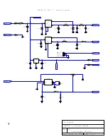
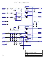
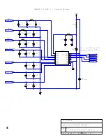
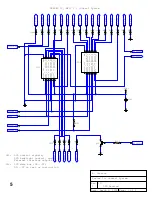
supply, interface, signal processing, display, and microcontroller. Schematics are found later in this
section.
Power Supply Components
There are (4) power supply voltages generated on the Series II – rev I PCB:
1. +5Vdc for all logic and general purpose PCB supply voltage
2. +4Vdc for the LED backlighting on the LCD
3. -4Vdc for the contrast voltage required by the LCD
4. +5Vdc for the directional coupler supply
The +5Vdc is generated from a small switching power supply comprised of C101, C102, D102,
L101, and U101. This power supply accepts DC input voltages up to 40Vdc (unless U101 is an HV
option, then the maximum input voltage is +60Vdc) and o5Vdc at up to 1Adc. This voltage is
always on, as the ON/OFF pin on U101 is hard-wired to the ‘on’ configuration. C103, L102, and
C104 form a noise choke to help filter out switching noise or RF noise that may radiate onto the
control circuit board.
The +4Vdc is generated from a small switching power supply comprised of components C105,
C106, D103, L103, and U102. This power supply accepts DC input voltages up to +40Vdc (unless
U102 is an HV option, then the maximum input voltage is 60Vdc) and o5Vdc at up to 1Adc.
The voltage then gets dropped down to +4Vdc through R101. This backlight voltage can be turned
on and off via the ON/OFF pin on U102. The PCB is designed in a manner that allows this voltage to
be hard-wired on all the time or controlled from the microcontroller through latch U111. This
selection is made with jumper J102.
The -4Vdc is generated using a switched capacitor voltage converter design, using components
C109, C110, R102, R103, U104, and VR101. U4 a5Vdc from the general p5Vdc
supply and generates -5Vdc. This voltage then gets dropped across the voltage divider (R102,
R103) to generate the contrast voltage specific to the LCD that is installed in the system.
Содержание TAV-500
Страница 1: ...TAV 500 POWER AMPLIFIER NEW ADVENTURES IN BROADCASTING Technalogix ...
Страница 17: ...A A 1 1 TECHNALOGIX LTD 25 W VHF LO BAND DRIVER P25 VHF L R S MCDONALD 14 SEPTEMBER 2000 ...
Страница 18: ...Technalogix Ltd 25 Watt High Band VHF Pallet PA25 VHF H S Kazarian November 12 2001 B B ...
Страница 19: ......
Страница 20: ...Technalogix Ltd 400 Watt High Band VHF Pallet P400 VHF H R S McDonald July 30 2001 B A ...
Страница 49: ...Technalogix Ltd VIII 9 Location and Function of Controls and Connectors Power Supply ...
Страница 57: ...Thank you for choosing Technalogix Ltd ...


