7
IC DESCRIPTIONS AND INTERNAL BLOCK DIAGRAM
n
TDA8840/8842/8844
n
TUNER (UV1315, UV1316, UV1336)
n
TEA6415C
n
TDA9830
n
TDA2614/2615/2616Q
n
TDA8351/8356
n
TDA6108M
n
TDA9181
n
TDA 44608
n
SDA555X
n
MSP34X0D
n
TDA4470
n
ST24C08
n
TDA1308
n
G1965M
n
TDA3430G
n
DPL3519A
n
SDA9488A
n
TDA9886
TDA8840/8842/8844:
The TDA884X is I²C-bus controlled single chip TV processor which is intended to be applied in PAL, NTSC, PAL/NTSC and
multi-standard television receivers. These IC s are nearly pin compatible with the TDA837X TV processors but have a higher
degree of integration because the delay line (TDA4665 function) and the SECAM decoder have been integrated. In addition to
these functions some additional features have been added like Continuous Cathode Calibration (2-point black current loop
which results in an accurate biasing of the 3 guns), adjustable luminance delay time, blue stretching and dynamic skin tone control.
Features:
n
Vision IF circuit with PLL demodulator
n
Alignment-free multi-standard FM sound demodulator (4.5 MHz to 6.5 MHz)
n
Audio switch
n
Flexible source selection with CVBS switch and Y(CVBS)/C input so that a comb filter can be applied
n
Integrated chrominance trap circuit
n
Integrated luminance delay line
n
Asymmetrical peaking in the luminance channel with a noise coring function
n
Black stretching of non-standard CVBS or luminance signals
n
Integrated chroma band-pass filter with switchable center frequency
n
Blue stretch circuit which offsets colours near white towards blue
n
RGB control circuit with Continuous Cathode Calibration and white point adjustment
n
Linear RGB inputs and fast blanking
n
Possibility to insert a blue black option when no video signal is available
n
Horizontal synchronisation with two control loops and alignment-free horizontal oscillator
n
Vertical count-down circuit
n
Vertical driver optimised for DC-coupled vertical output stages
n
I²C-bus control of various functions
n
Low dissipation (850 mW)
Functional Differences between the 8840/8842/8844:
IC VERSION (TDA)
8840
8842
8844
Multi-standard IF
X
X
Automatic Volume Limiting
X
X
PAL Decoder
X
X
X
SECAM Decoder
X
X
NTSC Decoder
X
X
Dynamic Skin Control
X
Colour Matrix PAL/NTSC (Japan)
X
X
Colour Matrix NTSC Japan/USA
YUV interface
X
Base-band delay line
X
X
X
Adjustable luminance delay time
X
Horizontal geometry
X
Horizontal and vertical zoom
X
Vertical scroll
X
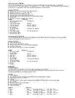
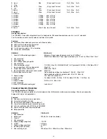
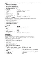
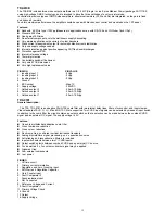
PINNING
PIN VALUE
1. Sound IF input
: 1mVrms
2. External audio input
: 500mVrms
3. IF demodulator tuned circuit 1
4. IF demodulator tuned circuit 2
5. IF-PLL loop filter
: Min:32-Max:60 MHz
6. IF video output
: 4.7V (Negative Modulation), 2V (Positive Modulation)
7. Serial clock input
: Low level max:1.5 V, High level min 3.5V
8. Serial data input/output
: Low level max:1.5 V, High level min 3.5V
9. Bandgap decoupling
10. Chrominance input (S-VHS)
: 1Vpp, Max:1.4Vpp
11. External CVBS/Y input
: 1Vpp, Max:1.4Vpp
12. Main supply voltage 1
: 8V, Min:7.2V, Max:8.8V
13. Internal CVBS input
: 1Vpp, Max:1.4Vpp
14. Ground 1
Содержание CTW2850
Страница 1: ...SERVICE MANUAL CTW2850 28 WIDE CTV Effective FEB02 CTW2850SERV ...
Страница 39: ...38 GENERAL BLOCK DIAGRAM OF CHASSIS AK19PRO ...
Страница 54: ......


