background image

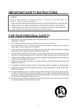
CA UT ION : T O RE DUCE

TH E RIS K OF

ELECTR ICA L SHOCK, DO NOT RE MOVE
COVER (OR BACK). NO USER SERVIC EABLE
PAR TS INS IDE . RE FE R SE R VIC ING TO
QUALIFIE D SERVICE PERSONNEL.

The lighting flash with arrowhead symbol, with an equilateral triangle is intended to
alert the user to the presence of uninsulated

voltage within the products

enclosure that may be of sufficient magnitude to constitute a risk of electric shock to
the person.

The exclamation point within an equilateral triangle is intended to alert the user to the
presence of important operating and maintenance (servicing) instructions in the
literature accompanying the appliance.

CA UTION:

Use of controls, adjustments or procedures other than those specified herein may result in
hazardous radiation exposure.

CA U T ION

RISK

RISK OF ELECTR I

ELECTR IC

SHOCK

SHOCK DO NOT

NOT OPEN.

OPEN.

2

dangerous

WARNING: TO REDUCE RISK OF FIRE OR ELECTRIC SHOCK, DO NOT

                      EXPOSE THIS APPLIANCE TO RAIN OR MOISTURE.

SCHNEIDER ELECTRONICS GMBH-GERMANY

1. CAUTION

Содержание L40B2800

Страница 1: ...ĂĂĂĂĂĂĂĂĂĂĂĂĂĂĂĂ2 5 Scheme DiagramĂĂĂĂĂĂĂĂĂĂĂĂĂĂĂĂĂĂĂĂĂĂĂ 2 6 PCB Layout ĂĂĂĂĂĂĂĂĂĂĂĂĂĂĂĂĂĂĂĂĂĂĂĂĂ27 7 Trouble ShootingĂĂĂĂĂĂĂĂĂĂĂĂĂĂĂĂĂĂĂĂĂĂĂĂ 8 Explode DiagramĂĂĂĂĂĂĂĂĂĂĂĂĂĂĂĂĂĂĂĂĂĂĂĂ35 9ˊBOM ListĂĂĂĂĂĂĂĂĂĂĂĂĂĂĂĂĂĂĂĂĂĂĂĂĂĂĂ36 This manual is the latest at the time of printing and does not include the modification which may be made after the printing by the constant improvement of product ...

Страница 2: ...electric shock to the person The exclamation point within an equilateral triangle is intended to alert the user to the presence of important operating and maintenance servicing instructions in the literature accompanying the appliance CAUTION Use of controls adjustments or procedures other than those specified herein may result in hazardous radiation exposure CA U T ION RISK RISK OF ELECTRI ELECTR...

Страница 3: ...o impact of any kind Be particularly careful not to damage the picture tube surface 9 Unplug this television set from the wall outlet before cleaning Do not use liquid cleaners or aerosol cleaners Use a damp cloth for cleaning 10 1 Do not place this television set on an unstable cart stand or table The television set may fall causing serious injury to a child or an adult and serious damage to the ...

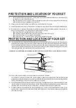
Страница 4: ...ing conductors location of antenna discharge unit connection to grounding electrode and requirements for the grounding electrode 15 2 Note to CATV system installer Only for the television set with CATV reception This reminder is provided to call the CATV system attention to Article 820 40 of the NEC that provides guidelines for proper grounding and in particular specifies that the cable ground sha...

Страница 5: ...edurein youroperatinginstructions do not attempt any further adjustment Unplug the set and call your dealer or service technician 22 Whenever the television set is damaged or fails or a distinct change in performance indicates a need for service unplug the set and have it checked by a professional service technician 23 It is normal for some TV sets to make occasional snapping or popping sounds par...

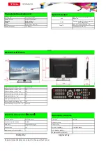
Страница 6: ...Time Typ 30 000hrs Subtitle Color 16 7M 8 bit Parental Control Yes at DTV Refresh Rate 60Hz Content restriction Yes at DTV Sleep Timer Yes System Update Yes Side Hotel Mode Input Method Smart TV IME MHL Teletext Nicam Lightsensor 3DTV Type 3D Format Natura Light Technology Yes Natural Light Engine DCC Dynamic Contrast Control ON Off Backlight Adjustable Yes 0 100 Color Temperature Normal Cold Warm...

Страница 7: ... 7 0 Gross Weight With Packaging Kg 10 8 VESA Mounting Dimensions LxH mm 100x150 Essential Accessories Default Operation Manual Spanish Default Wall Mount WMB333 Remote Control and batteries RC199C Wireless Keyboard Base Stand Integrated Packaging Wireless Mouse AC power cord 1 pc Built in WI FI AR9271 07 WF75RL MA0G Adapt Cable Wire For AV Or YPBPR WI FI DONGLE AR9271 RF Converter IECType toType ...

Страница 8: ...est Alignment Specification For MS08P LA Series V1 0 Page 1 of 9 7CL 3 R D CENTER Factory Test Alignment Specification FTAS for MS083 LA Series Version 1 PREPARED BY Hongxin Gao DATE 2014 04 23 APPROVED BY DATE ...

Страница 9: ... Disclosure The information contained in this document is proprietary to TCL IPC R D CENTER and shall not be disclosed by the recipient to third persons without the written permission of the team leader or GM of R D Revision History Version Issue Date Description of changes ...

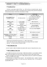
Страница 10: ...IF output Coaxial OAD No WIFI Yes DIVX No DLNA DMP Yes Internet Yes 3D auto top bottom side by side frame sequencing 1920x2205 24Hz 1920x1080p x2 1280x1470 50Hz 1280x720p x2 1280x1470 60Hz 1280x720p x2 Optional Functions Audio Return Channel ARC Yes I2C connector of MEMC module N A Others Main SW Serial NAND Flash BIN image U501 IC Details Position Main IC U700 INFO ª All tests and measurements me...

Страница 11: ...for amplifier AMP_VCC etc Position Value Remark UD90 5V 5 UD60 1 15V 5 U172 U175 3 3V 5 U174 1 5V 5 U201 TUNER_3 3V 1 2 SW Image download Developing Download the latest release SW from below PDM system Link http sw tcl cctv com Username Password See Appendix o How to upgrade FLASH SW using USB 1 3 Project ID Modification There are different ID stored into the NVM depending on dif ferent Panels set...

Страница 12: ...720i 60Hz RJ45 LAN Internet ICMP packets echo request Headphone via mini jack adapter RF signal Suitable channel Loud Speakers Enclosures RF signal Suitable channel AV OUT Audio RF signal Suitable channel Audio tones can be defined by the factory i e 1 KHz 3 KHz sweep Picture video formats can be changed by the factory according to their own standard Remark 1 AV Video Audio in shared with CMP 1 5 ...

Страница 13: ...y to pop up again the Factory menu The status of Factory Key can be changed in Factory Menu Hotkey Press RCU OK key or RIGHT key to enter the submenu Press RCU Menu key to go back to the root menu Press RCU RIGHT or LEFT key to change the values Press RCU OK key run the function Press RCU Exit key exit the Factory menu See Appendix t Factory Menu Description 2 2 Warm up Following TCL standard and ...

Страница 14: ... s RCU MENUÆSettingÆ Software upgradeÆBy USBÆConfirm Or turn of f the TV press and hold th e power key of key boar d before r econnect AC cord to restart TV for 5 8seconds Forced Upgrade When the UPGRADING SOFTW ARE picture appears as below it means TV is uploading SW BIN image Waiting a few minutes When updating is successful TV should restart automatically Appendix p How to change Project ID wit...

Страница 15: ... mode R Gain 000 255 R White balance 127 128 for gain G Gain 000 255 G White balance 127 128 for gain B Gain 000 255 B White balance 127 128 for gain R Offset 000 255 R G ray balance 127 128 for offset G Offset 000 255 G G ray balance 127 128 for offset B Offset 000 255 B G ray balance 127 128 for offset White Balance Init DO Press OK key to initial the preset RGB Gain Offset value VGA ADC Status ...

Страница 16: ...NVM CH list Upgrade Upgrade CH list USB UPDATE CH list backup Backup CH list 9 Device ID test submenu Item Sub item Value Note USB Clone Mode All Channel List EEPROM User Setting Select to c hoose th e th ings y ou want to clone TV TO USB DO Press R ight key to c opy the d ata WB ADC picture setting etc to USB USB Clone USB TO TV DO Press Right key to set the data WB ADC picture setting from USB A...

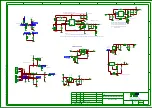
Страница 17: ...hange RD90 to adjust Fsw Set Fsw 600kHZ Vin 3V 36V Fixed OCP 5 5A Vref 0 8V If Input Voltage 12V CD90 CD91 10uF 16V NO 28 CC0106 KBX RD93 22K 3_3VSB 3_3VSB SWITCH POWER HI Panel ON Fixed Fsw 1 2MHZ For timing sequence BOM COST 1 22RMB C107 470P R110 10R DD91 SK54 C65 0 1U CD60 0 1U 1 2 3 4 5 P104 1 2 3 4 P103 R105 220R CD99 10U 7 8 4 2 3 5 6 1 Q101 PMK50XP 2 3 1 U174 AZ1117 DIM_OUT B C E Q102 BT39...

Страница 18: ...nter 6 11 10 7 8 1 3 2 4 5 9 TU101 1 2 3 4 U201 AZ1117 R205 1K TU1_VCC 5V 0 1U C216 C215 0 1U C214 10U 10V C217 220U 6 3V C207 0 022U R207 0R R208 10K 3_3V IF AGC TU_VCC T_SDA RF_SW R206 470R C203 10U R204 4K7 R203 4K7 AGC R202 33R C206 6800P R201 33R C201 22P C202 22P C205 22P C204 22P T_SDA IF IF TU1_VCC TU1_SCL RF_SW IF_AGC TU1_SDA T_SDA T_SCL TUNER_FAT TUNER_FAT TUNER_AGC TU1_VCC C209 0 1U C21...

Страница 19: ..._1 TXVP_0 TXVN_0 RXVP_1 C389 560P R389 12K C390 560P 10U C329 F321 R362 120R R361 220R C352 33P C351 0 1U R315 33R C303 0 047U R_IN L_IN AV YPBPR_R_IN AV YPBPR_L_IN C301 2U2 R305 10K F306 VCOM0 AV1_V_IN HD1_Y_IN HD1_PR_IN HD1_PB_IN C343 0 047U HD1_SOG_IN HD1_PB HD1_PR F313 R346 47R C344 0 047U R344 47R R348 75R R347 75R AV1 Y C330 0 047U R357 68R R343 68R C341 0 047U R342 75R R341 10R C345 1000P 0...

Страница 20: ...6 1 3 10 12 18 P802 AVDD5V_MHL R459 33R H2_HPD_OUT H2_HPD C410 2U2 H1_ARC R407 1K R416 100R R415 100R R404 100R R417 47K R429 47K H2_5V R434 5R6 15 16 2 5 8 11 17 19 13 14 7 9 4 6 1 3 10 12 18 P800 H1_HPD H1_RXC H1_RXC H1_RX0 H1_RX0 H1_RX1 H1_RX1 H1_RX2 H1_RX2 H_CEC H_CEC CEC F403 C401 0 047U R436 300K R435 100R MHL_CABLE_DET MHL_DETECT H2_5V R433 100R R432 100R H2_RX2 H2_RX0 H2_RX1 H2_RX2 H2_RX1 ...

Страница 21: ... 5V R516 27K 56K R515 R504 NC 10K SDI SCK WP DO CS MCU_RESET C501 0 1U NC 3_3VSB 3_3VSB 12V R511 3K3 47K R508 C502 NC 0 1U R507 47K R520 22R R521 22R PANEL_ON MS_DIM_OUT 3_3V 3_3V NAND_D7 NAND_CLE NAND_ALE NAND_DQS NAND D1 NAND D0 NAND_REZ C516 0 1U 2U2 C517 2U2 C503 C507 0 1U R523 22R PANEL_VCC C515 0 1U 0 1U C514 B C E Q506 BT3904 G D S Q505 PMV65XP C508 0 1U 2 3 1 0BAV99 D502 C E B BT3906 Q502 ...

Страница 22: ... X24M1 24M R604 NC 1M AUVAG POWER_DET R624 100K R623 1K R622 1M R620 100K AUVRM C642 33P C603 0 47U C602 0 1U C643 33P XTALO XTALI AVDD_DMPLL AVDD_AU C606 0 1U C610 0 1U NC C611 0 1U NC C612 0 1U NC C613 0 1U C604 2U2 C607 0 1U C608 0 1U C609 10U NC C615 10U C616 2U2 C617 0 1U C618 0 1U C619 0 1U C621 0 1U NC C620 0 1U NC C623 0 1U C625 0 1U C627 0 1U NC C629 0 1U C630 0 1U NC C628 0 1U NC C622 10...

Страница 23: ...DDR_DATA0_2 AVDD_DDR_DATA0_3 AVDD5V_MHL_D AVDD_AU33 AVDD_DVI_USB_MPLL AVDD_DVI_USB_MPLL1 AVDD_NODIE AVDD3P3_DMPLL VDDC11 GND59 GND60 GND61 GND62 GND63 GND64 GND65 GND66 GND67 GND68 GND69 GND70 GND71 GND72 GND73 GND74 GND75 AVDD_DDR_CMD0_1 MCP close to SOC J4 J8 J16 J17 K8 A14 B14 C13 C14 E14 F13 G9 K9 A13 H11 B13 H10 H7 M8 M10 N10 N9 A17 B17 R13 H18 H8 H6 G7 G8 G15 G18 E15 E18 F15 F18 C15 C18 D15 ...

Страница 24: ...808 1U C807 R817 10R OUTLN OUTRP OUTRN 1U C836 C813 330P C812 0 22U R828 10R R811 100R L802 220R NC R813 10K C826 0 1U C811 0 1U C825 1000P C810 1000P L806 22UH L803 22UH L801 22UH L808 22UH C822 0 1U C821 0 1U C817 0 1U C824 330P C820 330P R829 100K C809 1000P C804 1000P 1U C806 R815 100R R814 10K 1U C805 1U C803 R812 10R 1K R810 L807 220R NC L805 220R NC L804 220R NC C823 0 22U C819 0 22U C818 0...

Страница 25: ...00 1K 2 3 1 D100 MBR10100 R102 10K C104 0 1U C103 470U 35V L100 0 8UH 35V 470U C102 C101 470U 35V C100 1000P R101 22R R100 22R ZD501 6V8 ZD500 6V8 R504 10K C504 0 1U C503 470U 35V C502 470U 35V C501 1000P R503 22R R502 22R R501 22R D500 MUR460 B C E Q3 BT3904 ZD2 6V8 1 2 3 4 HS1 2 4 1 3 5 12 11 10 9 8 7 6 T1 D6 FR107 C10 220P D5 RL255 R16 33R R15 33R C6 2200P R14 120K C7 100P R18 0 22 R17 0 22 R20...

Страница 26: ... no picture Check the voltage of pin s of q208 2 1 Replace R270 and R271 Check the output of Q208 2 1 Check the voltage of g of Q208 OR replace Q208 Measure the wave of LVDS signal 1 2 Replace panel Check the supply of U201 ...

Страница 27: ...he wave of pin 8 9 of U1 1 Check the voltage of pin 6 7 of u1 OK Replace u1 Check the circuit between U1 and U201 Check the U201 measure the wave of SDA and SCL 1 repair the circuit of U101 and Q102 OK OK 1 Check the U201 OK ...

Страница 28: ... Check the components between VGA YPbPr port and U201 1 Replace the bad VGA YPbPr no picture OK Check the components between VGA YPbPr port and U201 1 Replace the bad Software of U202 ok 1 Check U201 ok OK OK 1 Replace the bad Replace U201 1 Replace the bad Check the peripheral components of U201 ...

Страница 29: ...pin 3 13 of U602 2 1 Repair the 12v supply Check the pin 6 of u602 2 1 Check q607 q608 q609 1 2 Replace U602 or replace the wire of speaker check u601 and volume control Check the wave of PIN 4 12 of U602 Check the pin 7 of u602 2 1 repair R691 and R692 ...

Страница 30: ...andby 5 0VSB OK 5 0V NG Check the voltage of pin s of q305 2 1 Check before Q305 Check the output of Q305 2 1 Check the voltage of g of Q305 OR replace Q305 Check U303 U304 short to Gnd 1 Replace the bad ...

Страница 31: ...The picture bad Replace the wire from P202A to t com Replace panel Replace the chassis NG Check the circuit between p202a and U201 Upgrade the software NG OK OK ...

Страница 32: ......

Страница 33: ...2V 85A 5MA SEC W D930 T8 40LAZ6 MA2 09 MM1Z33 DTX D ZENER SMD 33V 0 1A 0 5W MM1Z33 ZD951 T8 40LAZ6 MA2 09 MM1Z33 DTX D ZENER SMD 33V 0 1A 0 5W MM1Z33 ZD950 T8 40LAZ6 MA2 10 0FR104 FBX DIODE FR104 FAST RECTIFIER D902 T8 40LAZ6 MA2 10 0FR207 FBX D VC 2A 1000V 1 3V 50UA 60A 250NSEC W F D901 T8 40LAZ6 MA2 10 0RL255 EBX D PIN 1 1V 2_A 800V W DO 15 RL255 D91 T8 40LAZ6 MA2 10 0RL255 EBX D PIN 1 1V 2_A 80...

Страница 34: ... 0603 R973 T8 40LAZ6 MA2 19 AB0104 JTX SMD RES 100K OHM 1 10W 0603 RD92 T8 40LAZ6 MA2 19 AB0104 JTX SMD RES 100K OHM 1 10W 0603 R974 T8 40LAZ6 MA2 19 AB0104 JTX SMD RES 100K OHM 1 10W 0603 R972 T8 40LAZ6 MA2 19 AB0121 JTX SMD RES 5 120OHM1 10W 0603 R362 T8 40LAZ6 MA2 19 AB0153 FTX RES SMD 15K OHM 1 10W 1 0603 R990A T8 40LAZ6 MA2 19 AB0123 JTX SMD RES 12K OHM 1 10W 5 0603 R389 T8 40LAZ6 MA2 19 AB01...

Страница 35: ...RES 1000K OHM 1 8W 1 R989 T8 40LAZ6 MA2 19 BC0105 JTX SMD RES 0805 1 8W 5 1MΩ R994 T8 40LAZ6 MA2 19 BC0105 JTX SMD RES 0805 1 8W 5 1MΩ R993 T8 40LAZ6 MA2 19 BC0105 JTX SMD RES 0805 1 8W 5 1MΩ R992 T8 40LAZ6 MA2 19 BC0105 JTX SMD RES 0805 1 8W 5 1MΩ R991 T8 40LAZ6 MA2 19 BC0202 JTX SMD RES 2K OHM 1 8W 5 R934 T8 40LAZ6 MA2 19 BC0220 JTX SMD RES 0805 1 8W 5 22Ω R917 T8 40LAZ6 MA2 19 BC0220 JTX SMD RE...

Страница 36: ... GA0101 JTX SMD RES 100 OHM 1 16W 5 R416 T8 40LAZ6 MA2 19 GA0101 JTX SMD RES 100 OHM 1 16W 5 R351 T8 40LAZ6 MA2 19 GA0101 JTX SMD RES 100 OHM 1 16W 5 R585 T8 40LAZ6 MA2 19 GA0101 JTX SMD RES 100 OHM 1 16W 5 R404 T8 40LAZ6 MA2 19 GA0101 JTX SMD RES 100 OHM 1 16W 5 R815 T8 40LAZ6 MA2 19 GA0101 JTX SMD RES 100 OHM 1 16W 5 R811 T8 40LAZ6 MA2 19 GA0101 JTX SMD RES 100 OHM 1 16W 5 R352 T8 40LAZ6 MA2 19 ...

Страница 37: ...220K0OHM 5 1 16W 0402 R809 T8 40LAZ6 MA2 19 GA0224 JTX R SMD 220K0OHM 5 1 16W 0402 R335 T8 40LAZ6 MA2 19 GA0224 JTX R SMD 220K0OHM 5 1 16W 0402 R301 T8 40LAZ6 MA2 19 GA0229 JTX SMD RES 1 16W 2 2 OHM 5 R392 T8 40LAZ6 MA2 19 GA0229 JTX SMD RES 1 16W 2 2 OHM 5 R391 T8 40LAZ6 MA2 19 GA0229 JTX SMD RES 1 16W 2 2 OHM 5 R393 T8 40LAZ6 MA2 19 GA0229 JTX SMD RES 1 16W 2 2 OHM 5 R394 T8 40LAZ6 MA2 19 GA0229...

Страница 38: ...Y1 250V CY91 T8 40LAZ6 MA2 26 APL102 ME7S 1000PF 20 250V UN UNPPM CT7 Y1 250V CY92 T8 40LAZ6 MA2 27 AQK224 KV3T 0 22UF 10 AC250V 0 1 C42P2224K6SC00 CX91 T8 40LAZ6 MA2 27 MHB222 J0X FILM CAPACITOR 0 0000000022F 5 400V 0 0 C908 T8 40LAZ6 MA2 28 AA0225 KBX CAP CER SMD 2U2F 10V DCV 0603 C302 T8 40LAZ6 MA2 28 AA0225 KBX CAP CER SMD 2U2F 10V DCV 0603 C301 T8 40LAZ6 MA2 28 AA0225 KBX CAP CER SMD 2U2F 10V...

Страница 39: ...1NF 50 0V 0805 10 R Y C903 T8 40LAZ6 MA2 28 BB0102 KBX CAP CER SMD 1NF 50 0V 0805 10 R Y C978 T8 40LAZ6 MA2 28 BB0103 KBX CAP CER SMD 10NF 50 0V 0805 10 R Y C902 T8 40LAZ6 MA2 28 BB0104 KBX CAP CER SMD 100N0F 50V DCV 0805 C953B T8 40LAZ6 MA2 28 BB0104 KBX CAP CER SMD 100N0F 50V DCV 0805 C953A T8 40LAZ6 MA2 28 BB0104 KBX CAP CER SMD 100N0F 50V DCV 0805 C901 T8 40LAZ6 MA2 28 BB0104 KBX CAP CER SMD 1...

Страница 40: ...0402 C810 T8 40LAZ6 MA2 28 HB0103 KBX CAP CER SMD 10N0F 50V DCV 0402 C103 T8 40LAZ6 MA2 28 HB0103 KBX CAP CER SMD 10N0F 50V DCV 0402 C102 T8 40LAZ6 MA2 28 HB0103 KBX CAP CER SMD 10N0F 50V DCV 0402 C106 T8 40LAZ6 MA2 28 HB0220 JCX CAP CER SMD 22P0F 50V DCV 0402 C201 T8 40LAZ6 MA2 28 HB0220 JCX CAP CER SMD 22P0F 50V DCV 0402 C202 T8 40LAZ6 MA2 28 HB0220 JCX CAP CER SMD 22P0F 50V DCV 0402 C205 T8 40L...

Страница 41: ...2 28 HC0104 KBX CAP CER SMD 100NF 16V 0402 C610 T8 40LAZ6 MA2 28 HC0104 KBX CAP CER SMD 100NF 16V 0402 C626 T8 40LAZ6 MA2 28 HC0104 KBX CAP CER SMD 100NF 16V 0402 C611 T8 40LAZ6 MA2 28 HC0104 KBX CAP CER SMD 100NF 16V 0402 C627 T8 40LAZ6 MA2 28 HC0104 KBX CAP CER SMD 100NF 16V 0402 C628 T8 40LAZ6 MA2 28 HC0104 KBX CAP CER SMD 100NF 16V 0402 C324 T8 40LAZ6 MA2 28 HC0104 KBX CAP CER SMD 100NF 16V 04...

Страница 42: ...ES 4 7K OHM 1 16W 5 R208 T8 40LAZ6 MA2 19 AB0104 JTX SMD RES 100K OHM 1 10W 0603 R979A T8 40LAZ6 MA2 19 AB0000 JTX RES SMD 0 OHM 1 10W 5 0603 R979B T8 40LAZ6 MA2 19 GA0101 JTX SMD RES 100 OHM 1 16W 5 R440 T8 40LAZ6 MA2 19 GA0103 JTX SMD RES 10K OHM 1 16W 5 R439 T8 40LAZ6 MA2 33 NLL109 NTXCKI IND SMD 22UH 20 1 7A SLF5020 100MOHM LD60 T8 40LAZ6 MA2 33 NLL220 MTXCKI IND SMD 22UH 20 1 7A SLF5020 100MO...

Страница 43: ...R WIRE 1000MM 5PIN PH LOCK GH 2 0 FOR IR BD T8 40B380Z6 RC2 62 980640 0HG6R DEC HOLDER VESA BOSS 00 00 R N T8 40B380Z6 RC2 63 B3012T BF5G SCREW ST 3MM 12MM ISO 19 R Y FOR S RC T8 40B380Z6 RC2 63 B4010T BF4G SCREW ST 4MM 10MM ISO R Y FOR VESA T8 40B380Z6 RC2 63 B4010T BF4G SCREW ST 4MM 10MM ISO R Y FOR 67 M5 T8 40B380Z6 RC2 64 B30050 105G SCREW 3MM 5MM M3X5 R Y FOR CHASS T8 40B380Z6 RC2 67 M47721 0...

Страница 44: ...471 FTX RES SMD 470 OHM 1 10W 1 0603 R5 T8 28B250KG KE2 19 AB0471 FTX RES SMD 470 OHM 1 10W 1 0603 R7 T8 28B250KG KE2 19 AB0471 FTX RES SMD 470 OHM 1 10W 1 0603 R1 T8 28B250KG KE2 48 TAC001 XX0 TACT SWITCH K3 T8 28B250KG KE2 48 TAC001 XX0 TACT SWITCH K6 T8 28B250KG KE2 48 TAC001 XX0 TACT SWITCH K1 T8 28B250KG KE2 48 TAC001 XX0 TACT SWITCH K7 T8 28B250KG KE2 48 TAC001 XX0 TACT SWITCH K2 T8 28B250KG...

Отзывы: