background image

1-4-2

DVD_NOTE

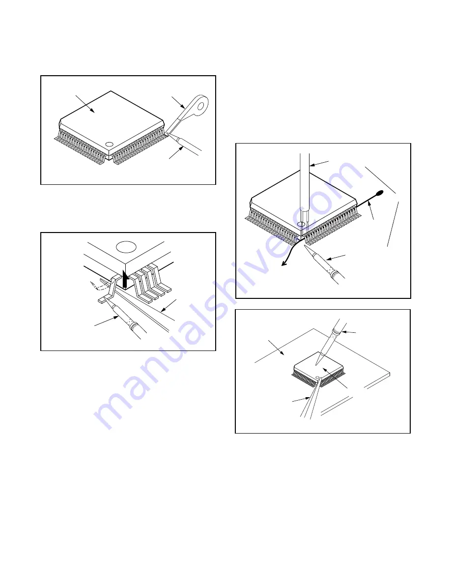
With Soldering Iron:

(1) Using desoldering braid, remove the solder from all

pins of the flat pack-IC. When you use solder flux
which is applied to all pins of the flat pack-IC, you
can remove it easily. (Fig. S-1-3)

(2) Lift each lead of the flat pack-IC upward one by

one, using a sharp pin or wire to which solder will
not adhere (iron wire). When heating the pins, use
a fine tip soldering iron or a hot air desoldering
machine. (Fig. S-1-4)

(3) Bottom of the flat pack-IC is fixed with glue to the

CBA; when removing entire flat pack-IC, first apply
soldering iron to center of the flat pack-IC and heat
up. Then remove (glue will be melted). (Fig. S-1-6)

(4) Release the flat pack-IC from the CBA using twee-

zers. (Fig. S-1-6)

With Iron Wire:

(1) Using desoldering braid, remove the solder from all

pins of the flat pack-IC. When you use solder flux
which is applied to all pins of the flat pack-IC, you
can remove it easily. (Fig. S-1-3)

(2) Affix the wire to a workbench or solid mounting

point, as shown in Fig. S-1-5.

(3) While heating the pins using a fine tip soldering

iron or hot air blower, pull up the wire as the solder
melts so as to lift the IC leads from the CBA contact
pads as shown in Fig. S-1-5

(4) Bottom of the flat pack-IC is fixed with glue to the

CBA; when removing entire flat pack-IC, first apply
soldering iron to center of the flat pack-IC and heat
up. Then remove (glue will be melted). (Fig. S-1-6)

(5) Release the flat pack-IC from the CBA using twee-

zers. (Fig. S-1-6)

Note:

When using a soldering iron, care must be taken
to ensure that the flat pack-IC is not being held by
glue. When the flat pack-IC is removed from the
CBA, handle it gently because it may be damaged
if force is applied.

Flat Pack-IC

Desoldering Braid

Soldering Iron

Fig. S-1-3

Fine Tip
Soldering Iron

Sharp
Pin

Fig. S-1-4

To Solid 
Mounting Point

Soldering Iron

Iron Wire

or

Hot Air Blower

Fig. S-1-5

Fine Tip
Soldering Iron

CBA

Flat Pack-IC

Tweezers

Fig. S-1-6

Содержание DVL100D

Страница 1: ...SERVICE MANUAL DVD PLAYER DVL100D ...

Страница 2: ...ssible hazardous consequences of each way Consequently Funai has not undertaken any such broad evaluation Accordingly a servicer who uses a service procedure or tool which is not recommended by Funai must first use all precautions thoroughly so that neither his safety nor the safe operation of the equipment will be jeopardized by the service method selected TABLE OF CONTENTS SPECIFICATIONS 1 1 1 L...

Страница 3: ... imp 100 K ohm 4 Room ambient 25 C ITEM CONDITIONS UNIT NOMINAL LIMIT 1 Video Output 75 ohm load Vpp 1 0 0 1 2 Coaxial Digital Out 75 ohm load mVpp 500 100 3 Audio PCM 3 1 Output Level 1kHz 0dB Vrms 2 0 3 2 S N dB 120 3 3 Freq Response DVD fs 48kHz 20 22kHz dB 0 5 CD fs 44 1kHz 20 20 kHz dB 0 5 3 4 THD N DVD 1 kHz 0dB 0 0025 CD 1 kHz 0dB 0 003 ...

Страница 4: ...tion shown in the figure When checking the laser diode be sure to keep your eyes at least 30cm away from the pickup lens when the diode is turned on Do not look directly at the laser beam Caution Use of controls and adjustments or doing procedures other than those specified herein may result in hazardous radiation exposure Do not look directly at the laser beam coming from the pickup or allow it t...

Страница 5: ...especially 1 Wires covered with PVC tubing 2 Double insulated wires 3 High voltage leads D Use specified insulating materials for hazardous live parts Note especially 1 Insulation tape 2 PVC tubing 3 Spacers 4 Insulators for transistors E When replacing AC primary side components transformers power cord etc wrap ends of wires securely about the terminals before solder ing F Observe that the wires ...

Страница 6: ...ference only Be sure to confirm the precise values 2 Leakage Current Test Confirm the specified or lower leakage current between B earth ground power cord plug prongs and externally exposed accessible parts RF termi nals antenna terminals video and audio input and output terminals microphone jacks earphone jacks etc is lower than or equal to the specified value in the table below Measuring Method ...

Страница 7: ...ve the flat pack IC with tweezers while apply ing the hot air 3 Bottom of the flat pack IC is fixed with glue to the CBA when removing entire flat pack IC first apply soldering iron to center of the flat pack IC and heat up Then remove glue will be melted Fig S 1 6 1 Release the flat pack IC from the CBA using twee zers Fig S 1 6 Caution 1 Do not supply hot air to the chip parts around the flat pa...

Страница 8: ...l pins of the flat pack IC you can remove it easily Fig S 1 3 2 Affix the wire to a workbench or solid mounting point as shown in Fig S 1 5 3 While heating the pins using a fine tip soldering iron or hot air blower pull up the wire as the solder melts so as to lift the IC leads from the CBA contact pads as shown in Fig S 1 5 4 Bottom of the flat pack IC is fixed with glue to the CBA when removing ...

Страница 9: ...ur due to a potential difference caused by electro static charge during unpacking or repair work 1 Ground for Human Body Be sure to wear a grounding band 1MΩ that is prop erly grounded to remove any static electricity that may be charged on the body 2 Ground for Workbench 4 Be sure to place a conductive sheet or copper plate with proper grounding 1MΩ on the workbench or other surface where the sem...

Страница 10: ...EO OUT connect to a TV with S Video inputs Caution Do not touch the inner pins of the jacks on the rear panel Electrostatic discharge may cause permanent damage to the player 9 PAUSE pause playback temporarily frame by frame playback 10 h h to view DVD picture in fast reverse motion 11 PLAY to start a DVD disc playback 12 SETUP to access or remove the DVD setup menu 13 MODE to set up programed or ...

Страница 11: ...rted disc is being played back Lights up when a CD is inserted on the tray Lights up when a DVD is inserted on the tray Lights up when the inserted disc comes to a pause Stays on when the A B repeat function is on Stays on when the repeat function is on Displays how long a current title or track has been played back When a chapter or track has switched the number of a new title chapter or track is...

Страница 12: ...this first release two Locking Tabs A at the side and then three Locking Tabs B at the bottom CAUTION 2 Electrostatic breakdown of the laser diode in the optical system block may occur as a potential difference caused by electrostatic charge accumulated on cloth human body etc during unpacking or repair work To avoid damage of pickup follow next procedures 2 1 Slide out the pickup unit as shown in...

Страница 13: ...ray Panel A A L 3 L 2 L 1 L 1 B Fig D2 3 DVD Mecha S 2 S 2 CN201 CN301 S 3 4 Front Shield Fig D3 View for A Pickup Unit B A Short the three short lands by soldering View for B Slide DVD Mecha Fig D4 5 AV CBA 6 DVD Main CBA Unit S 6 S 4 S 5 CN1601 CN1001 S 5 Fig D5 ...

Страница 14: ...DC S 7 7 Rear Panel S 8 8 Holder Fig D6 Rotate this roulette in the direction of the arrow A View for A HOW TO MANUAL EJECT 1 Remove the Top Case 2 Rotate the roulette in the direction of the arrow as shown below ...

Страница 15: ...Y MATRIX IC202 OP AMP 12 14 CN3002 CN301 FG CBA FG SENSOR M SLED MOTOR M SPINDLE MOTOR IC101 MICRO CONTROLLER SLED MOTOR DRIVE FOCUS ACTUATOR DRIVE 1 4 1 4 PLL2 X451 MULTI PLL X TAL OSC 36 864MHz OSC SPINDLE MOTOR DRIVE TRACKING ACTUATOR DRIVE EXT CLOCK CLK33M BE CLOCK 172 170 150 TRAY OUT TRAY IN FG IN 97 SLD 70 SPDL 71 TRACKING DRIVE 152 FOCUS DRIVE 60 66 TO DIGITAL SIGNAL PROCESS BLOCK DIAGRAM ...

Страница 16: ...RIAL D A GENERAL I O INTERRUPT CONTROLLER TIMER WATCH DOG TIMER 32BIT CPU STREAM I F EXTERNAL MEMORY I F SDRAM ECC UMAC 124 125 122 123 128 129 126 127 131 130 135 133 132 134 78 DEBUG BCU INST CACHE D TYPE LATCH DATA CACHE D A D A D A TO VIDEO AUDIO BLOCK DIAGRAM 158 164 Y C Cr Cb VIDEO Y VIDEO C VIDEO Cr VIDEO Cb TO VIDEO AUDIO BLOCK DIAGRAM 181 SPDIF 175 PCM BCK 176 PCM DATA0 174 PCM LRCLK 161 ...

Страница 17: ... DAC LPF AMP L CH R CH LPF AMP DAC ZERO DETECT SYSTEM CLOCK 1 2 6 7 5 AUDIO R OUT PCM BCK SPDIF PCM DATA0 PCM LRCLK ADAC MD ADAC MC ADAC ML PCM SCLK AV CBA DVD MAIN CBA UNIT AUDIO SIGNAL DATA AUDIO SIGNAL 16 16 SPDIF A MUTE 3 3V Q1204 WF6 3 WF4 WF5 CN601 5 5 VIDEO Y 7 7 VIDEO C 3 3 VIDEO Cb 1 1 VIDEO Cr VIDEO Y VIDEO C VIDEO Cb VIDEO Cr JK1401 S VIDEO OUT CN1601 3 4 2 1 IC1402 VIDEO DRIVER 18 4dB ...

Страница 18: ...003 Q1001 2 4 7 3 4 IC1001 ERROR VOLTAGE DET T1001 11 12 13 15 14 16 17 18 SWITCHING SWITCHING CONTROL 1 2 6 BRIDGE RECTIFIER HOT AV CBA A V F HOT CIRCUIT BE CAREFUL D1003 RECTIFIER D1006 RECTIFIER D1008 RECTIFIER D1030 D1015 RECTIFIER D1016 RECTIFIER Q1016 Q1006 Q1005 Q1011 Q1015 Q1002 CN1001 Q1004 FL EV 5V F2 F1 P ON 9V EV 3 3V P ON 5V P ON 3 3V TO CN401 1 2 3 EV 1 5V 4 5 EV 3 3V 14 15 EV 9V 13 ...

Страница 19: ... in the schematic diagram and the parts list Before replacing any of these components read the parts list in this manual carefully The use of substitute replacement parts that do not have the same safety characteristics as speci fied in the parts list may create shock fire or other hazards Notes 1 Do not use the part number shown on these draw ings for ordering The correct part number is shown in ...

Страница 20: ...ity of repaired units use only original replacement parts which are listed with their part numbers in the parts list section of the service manual 4 Wire Connectors 1 Prefix symbol CN means connector can disconnect and reconnect 2 Prefix symbol CL means wire solder holes of the PCB wire is soldered directly 5 Mode SP 6 Voltage indications for PLAY and STOP mode on the schematics are as shown below...

Страница 21: ...ACKING SERVO SIGNAL FOCUS SERVO SIGNAL SPINDLE SERVO SIGNAL SLED SERVO SIGNAL DVD Main 1 3 Schematic Diagram 1 8 3 1 8 4 E5700SCD1 DVD MAIN 1 3 Ref No Position IC201 B 1 IC202 E 4 IC301 D 3 IC461 E 1 Q251 C 2 Q252 B 2 Q253 C 2 Q254 B 2 CN201 A 3 CN301 A 1 CN401 F 3 CONNECTORS ICS TRANSISTORS ...

Страница 22: ...3 J4 K1 K2 K3 K4 L1 L2 L3 L4 DATA VIDEO AUDIO VIDEO SIGNAL FOCUS SERVO SIGNAL TRACKING SERVO SIGNAL SPINDLE SERVO SIGNAL SLED SERVO SIGNAL DATA AUDIO DVD Main 2 3 Schematic Diagram 1 8 5 1 8 6 E5700SCD2 DVD MAIN 2 3 Ref No Position IC101 H 4 IC ...

Страница 23: ...127 2 0 2 0 32 64 96 3 4 3 4 128 2 0 2 0 PIN NO PLAY STOP PIN NO PLAY STOP PIN NO PLAY STOP PIN NO PLAY STOP 129 2 0 2 0 161 0 5 0 5 193 225 1 9 1 9 130 2 2 2 2 162 1 4 1 4 194 0 0 226 3 3 3 3 131 2 3 2 3 163 195 3 3 3 3 227 132 0 4 0 1 164 0 9 0 9 196 228 133 1 2 0 4 165 3 3 3 3 197 229 134 0 4 0 1 166 1 5 1 5 198 0 0 230 0 0 135 0 2 0 2 167 0 0 199 231 136 2 3 2 3 168 2 1 2 1 200 232 3 3 3 3 137...

Страница 24: ...1 P2 P3 P4 Q1 Q2 Q3 Q4 R1 R2 R3 R4 VIDEO SIGNAL DATA AUDIO AUDIO SIGNAL DVD Main 3 3 Schematic Diagram 1 8 9 1 8 10 E5700SCD3 DVD MAIN 3 3 Ref No Position IC102 O 4 IC103 O 3 IC104 N 3 IC105 N 1 IC451 P 3 IC601 Q 1 CN601 R 2 ICS CONNECTOR ...

Страница 25: ... REPLACE FUSE AS MARKED This symbol means fast operating fuse Ce symbole reprèsente un fusible à fusion rapide AV 1 3 Ref No Position IC1001 B 1 IC1002 D 4 IC1006 C 1 Q1001 B 3 Q1002 D 3 Q1003 B 2 Q1004 D 3 Q1005 D 2 Q1006 D 1 Q1011 D 1 Q1015 D 2 Q1016 E 2 CN1001 F 4 ICS TRANSISTORS CONNECTOR CAUTION Fixed voltage or Auto voltage selectable power supply circuit is used in this unit If Main Fuse F0...

Страница 26: ...1 K2 K3 K4 L1 L2 L3 L4 VIDEO SIGNAL DATA AUDIO AUDIO SIGNAL AV 2 3 Schematic Diagram 1 8 13 1 8 14 E5700SCAV2 AV 2 3 Ref No Position IC1201 H 1 IC1402 I 3 Q1201 J 1 Q1202 J 1 Q1203 I 2 Q1204 I 1 Q1351 J 4 Q1352 H 2 CN1601 G 3 ICS TRANSISTORS CONNECTOR ...

Страница 27: ...g c b e f 1 3 2 4 5 DVD VCD PBC STANDBY A B REPEAT TRK CHP TITLE 7G 6G 5G 4G 3G 2G 1G a b c d e f g c d e f g c d e f g c d e f g c d e f g c d e f g h i a b a b a b a b a b FL2001 MATRIX CHART STANDBY TITLE CHP TRK CD V PBC DVD REPEAT A B 1 3 2 4 5 1 8 15 1 8 16 E5700SCAV3 AV 3 3 Ref No Position IC2001 O 3 IC ...

Страница 28: ...ION FOR CONTINUED PROTECTION AGAINST FIRE HAZARD REPLACE ONLY WITH THE SAME TYPE FUSE ATTENTION POUR UNE PROTECTION CONTINUE LES RISQES D INCELE N UTILISER QUE DES FUSIBLE DE MÊME TYPE RISK OF FIRE REPLACE FUSE AS MARKED This symbol means fast operating fuse Ce symbole reprèsente un fusible à fusion rapide CAUTION Fixed voltage or Auto voltage selectable power supply circuit is used in this unit I...

Страница 29: ...FUSE ATTENTION POUR UNE PROTECTION CONTINUE LES RISQES D INCELE N UTILISER QUE DES FUSIBLE DE MÊME TYPE RISK OF FIRE REPLACE FUSE AS MARKED This symbol means fast operating fuse Ce symbole reprèsente un fusible à fusion rapide CAUTION Fixed voltage or Auto voltage selectable power supply circuit is used in this unit If Main Fuse F001 is blown check to see that all components in the power supply ci...

Страница 30: ...TOP MODE WF1 WF3 WAVEFORMS WF6 SPDIF Pin 16 of CN1601 1V 0 1µsec WF1 Pin 5 of CN1601 WF3 Pin 21 of IC1402 WF4 AUDIO L Pin 11 of CN1601 1V 0 5msec WF5 AUDIO R Pin 13 of CN1601 1V 0 5msec WF2 Pin 7 of CN1601 VIDEO Y 0 2V 20µsec VIDEO C 0 2V 20µsec VIDEO CVBS 0 5V 20µsec ...

Страница 31: ...N1001 VIDEO Cr 1 1 GND 2 2 VIDEO Cb 3 3 A MUTE 10 10 GND 9 9 GND 4 4 VIDEO Y 5 5 GND 6 6 VIDEO C 7 7 GND 8 8 CN601 CN1601 AC CORD AUDIO OUT L AUDIO OUT R VIDEO OUT DIGITAL AUDIO OUT S VIDEO OUT EV 1 5V 3 3 DRIVE CBA VIDEO Y OUT VIDEO Cb OUT VIDEO Cr OUT SPDIF 16 16 AUDIO L 11 11 A L MUTE 12 12 AUDIO R 13 13 A R MUTE 14 14 AUDIO 5V 15 15 FS TS DETECTOR 11 2 3 5 6 4 7 FG CBA FG SENSOR TRAY OUT SW300...

Страница 32: ...et Then plug it again 7 Turn the power on by pressing the power button and the tray will close 8 Press 1 2 3 4 and DISPLAY buttons on the remote control unit in that order Fig g appears on the screen 9 Press 3 button on the remote control unit Fig h appears on the screen 10 To finish this mode press POWER button F W Version Up Mode Please insert a DISC for F W Version Up EXIT POWER Fig a Version U...

Страница 33: ...ray IN TL221 3 3V 0V 0V 3 3V 0V 1 65V 0V 0V 0V 1 65V 1 65V 1 65V Tray OUT TL220 Sled Drive TP303 Disc Drive TP301 Focus Drive TP304 Tracking Drive Tracking Drive TP302 Tray Close Disc Rotation Play Disc Stop Tray Open SYSTEM CONTROL TIMING CHARTS ...

Страница 34: ... 7 Out a KEY 1 Segment Output Key Source 1 8 Out b Key 2 Segment Output Key Source 2 9 Out c Key 3 Segment Output Key Source 3 10 Out d Key 4 Segment Output Key Source 4 11 Out e Segment Output 12 In f 13 In g 14 Out h 15 VEE Pull Down Level 16 Out i Segment Output 17 Out 7G Grid Output 18 6G 19 5G 20 4G 21 3G 22 2G 23 1G 24 VDD Power Supply 25 VSS GND 26 In OSC Oscillator Input 27 Out DOUT Serial...

Страница 35: ...98 Y 2SC2120 Y TPE2 E C B 2SC2785 H KTC3199 GR KRA110M KTA1267 Y BN1L3Z P A K C E LTV 817 B C F KIA431 AT G D S 2SK3374 PQ070XF01SZ K A R 1 2 3 4 Note A Anode K Cathode E Emitter C Collector B Base R Reference G Gate D Drain S Source 1 Vin 2 Vo 3 GND 4 Vc 24 13 12 MM1622XJBE 1 LEAD IDENTIFICATIONS ...

Страница 36: ...L011 2L011 2L011 A16 See Electrical Parts List for parts with this mark Some Ref Numbers are not in sequence AV CBA 2B3 2L031 2L105 2L101 F1001 W1601 W1001 2L031 1B1 AC1001 2L021 2L082 A2 2L021 2L021 JK1202 JK1401 A23 A13 A13 A21 A22 JK1404 2B24 2B21 2B24 EXPLODED VIEWS Cabinet ...

Страница 37: ...B0 15 B0 16 B0 14 B0 13 CN3001 MECHA CBA L0 8 Grease point of B0 17 Grease point on B1 5 View for A Top View Bottom View A Grease point on bottom of B1 1 Grease point on bottom of B1 8 Grease point on B1 5 View for B B Mark Description HANAL UD 38L5 FAG 102R DVD Mechanism ...

Страница 38: ...1 15 3 E5700EX X10 X5 X2 X4 S2 S2 S4 Unit S1 A22 X1 X36 Packing ...

Страница 39: ...HT M3X4 BIND HEAD GBMC3040 2L101 SCREW C TIGHT M3X6 BIND HEAD GBMC3060 2L105 P TIGHT SCREW 3X8 BIND GBMP3080 DVD MECHANISM 1B1 DVD MECHA 0838 VCDVM040 N79F0GVM MECHA CBA 0VSA13365 B0 13 GEAR B N79F0GVM 0VM203636 B0 14 GEAR C N79F0GVM 0VM305507 B0 15 GEAR D N79F0GVM 0VM305508 B0 16 GEAR E N79F0GVM 0VM305509 B0 17 PLATE TRIGGER N79F0GVM 0VM203633 B1 1 MAIN CHASSIS N79F0GVM 0VM101137 B1 2 CLAMPER N79...

Страница 40: ... CHD1JJ3CH221 C1206 CHIP CERAMIC CAP CH J 220pF 50V CHD1JJ3CH221 C1207 CHIP CERAMIC CAP CH J 47pF 50V CHD1JJ3CH470 C1208 CHIP CERAMIC CAP CH J 47pF 50V CHD1JJ3CH470 C1221 ELECTROLYTIC CAP 10µF 16V M CE1CMASDL100 C1222 ELECTROLYTIC CAP 10µF 16V M CE1CMASDL100 C1223 CHIP CERAMIC CAP 1608 CH J 1000pF 50V CHD1JJ3CH102 C1224 CHIP CERAMIC CAP 1608 CH J 1000pF 50V CHD1JJ3CH102 C1245 CHIP CERAMIC CAP F Z ...

Страница 41: ...1 INDUCTOR 0 47µH K 26T LLAXKATTUR47 L1401 CHIP RES 1608 1 10W 0 Ω RRXAZR5Z0000 Ref No Description Part No L1421 CHIP RES 1608 1 10W 0 Ω RRXAZR5Z0000 L1441 CHIP RES 1608 1 10W 0 Ω RRXAZR5Z0000 L1442 CHIP RES 1608 1 10W 0 Ω RRXAZR5Z0000 L1461 CHIP RES 1608 1 10W 0 Ω RRXAZR5Z0000 L1481 CHIP RES 1608 1 10W 0 Ω RRXAZR5Z0000 L1521 CHOKE COIL 22µH K LLBD00PKV006 L1522 PCB JUMPER D0 6 P5 0 JW5 0T L2001 P...

Страница 42: ... Ω RRXAJR5Z0104 R1240 CHIP RES 1608 1 10W J 100k Ω RRXAJR5Z0104 R1245 CHIP RES 1608 1 10W J 10 Ω RRXAJR5Z0100 R1351 CHIP RES 1608 1 10W J 1 8k Ω RRXAJR5Z0182 Ref No Description Part No R1352 CHIP RES 1608 1 10W J 2 2k Ω RRXAJR5Z0222 R1353 CHIP RES 1608 1 10W J 2 2k Ω RRXAJR5Z0222 R1354 CHIP RES 1608 1 10W J 220 Ω RRXAJR5Z0221 R1355 CHIP RES 1608 1 10W J 75 Ω RRXAJR5Z0750 R1356 CHIP RES 1608 1 10W ...

Страница 43: ... 1A 250V PAGG20CAG102 FH1001 FUSE HOLDER MSF 015 XH01Z00LY001 FH1002 FUSE HOLDER MSF 015 XH01Z00LY001 FL2001 V F D 20U29100SAN TVFD150FT007 JK1202 RCA JACK BLACK MSP 251V 01 NI JXRL010LY070 JK1401 S TYPE JACK MDC 050V 2 4 JXEL040LY001 JK1404 RCA JACK MSD 246V 65NI PBSN JXRL060LY069 RM2001 REMOTE RECEIVER PIC 37042LU USESJRSKK033 SA1001 SURGE ABSORBER PVR 10D471KB or NVQZ10D471KB SURGE ABSORBER CNR...

Страница 44: ...Printed in Japan 2002 12 20 HO DVL100D E5700UD ...

Отзывы: