background image

S

UPER X5DL8-GG/X5DLR-8G2+/X5DLR-8G2


User’s Manual

1-6

Introduction

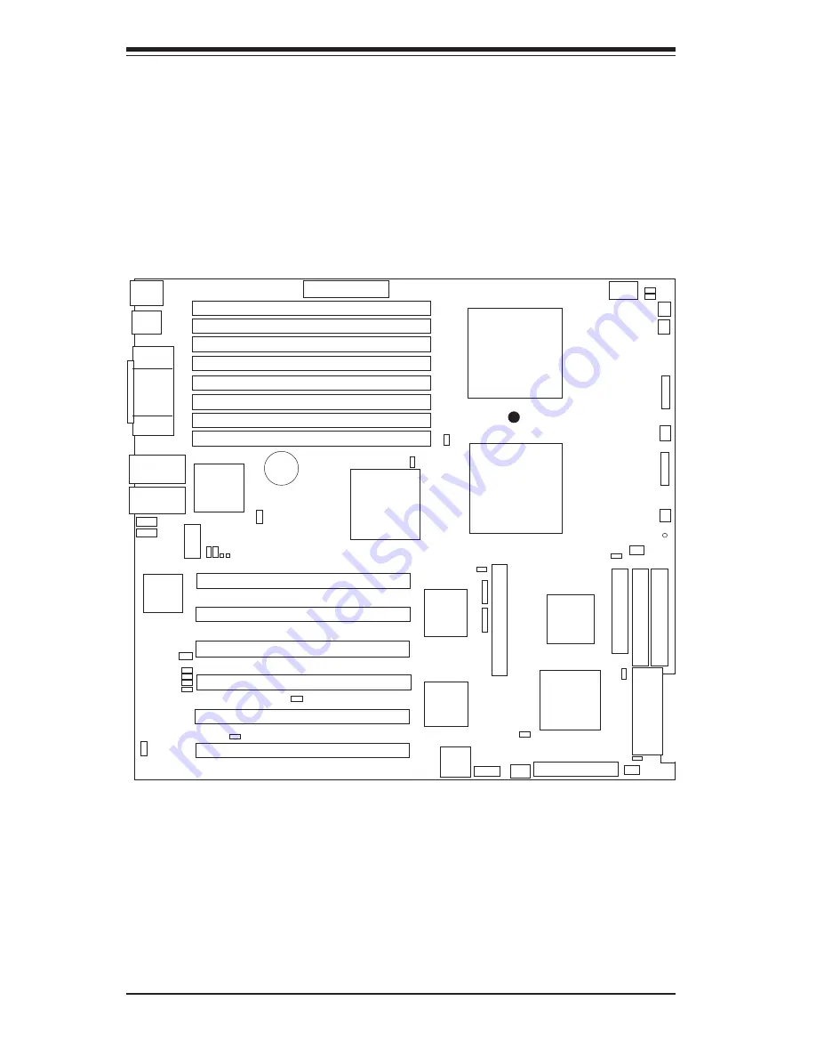
Figure 1-3.  SUPER X5DL8-GG Layout

(not drawn to scale)

Note: DIP Switch 4 sets the CPU Core/Bus Ratio (see Section 2-7).

  CR5 is a power LED indicator (see Section 2-6).

Jumpers not noted are for test purposes only.
IPMI is optional.

Also see Chapter 2 for the locations of the I/O ports and Front Control Panel

(JF1/JF2) connectors and for details on jumper settings and pin definitions.

123456789012345678901234

123456789012345678901234

123456789012345678901234

J11

Keyboard/Mouse

J66

ATX POWER

GLAN1

USB0/1

Rage XL

J55

COM1

VGA

GLAN2

CPU1

CPU2

North
Bridge

BATTERY

J56

Bank 1A

Bank 1B

Bank 2A

Bank 2B

Bank 3A

Bank 3B

Bank 4A

Bank 4B

Parallel

Port

J65

D5-D8

COM2

D1-D4

South
Bridge

Broadcom

Controller

S

UPER    X5DL8-GG

®

J12

J19

J18

IDE #2

IDE #1

FLOPPY

PCI-X #6

PCI-X #5

PCI-X #4

PCI-X #1

PCI-X #2

PCI-X #3

BIOS

AIC-7902

Ultra III LVD/SE ChB

IPMI

JP54

SW4

Ultra III LVD/SE ChA

IO Bridge

JF1

CPU2/CHS FAN

CPU2 FAN

CPU1 FAN

CPU1/CHS FAN

OH/CHS FAN

JF2

IO Bridge

JP48

JP7

JP4

JP56

JBT1

S1

P1

P2

S2

WOL

JP2

J29

J1

JA4

JPA1

CHS FAN

JPA2

CR5

JP58

JP57

J35

J20

J21

JP3

JA2

JA1

JP12

Содержание X5DL8-GG

Страница 1: ... SUPER X5DL8 GG SUPER X5DLR 8G2 SUPER X5DLR 8G2 USER S MANUAL Revision 1 0c SUPER ...

Страница 2: ...BILITY TO USE THIS PRODUCT OR DOCUMENTATION EVEN IF ADVISED OF THE POSSIBILITY OF SUCH DAMAGES IN PARTICULAR THE VENDOR SHALL NOT HAVE LIABILITY FOR ANY HARDWARE SOFTWARE OR DATA STORED OR USED WITH THE PRODUCT INCLUDING THE COSTS OF REPAIRING REPLACING INTEGRATING INSTALLING OR RECOVERING SUCH HARDWARE SOFTWARE OR DATA Any disputes arising between manufacturer and customer shall be governed by th...

Страница 3: ...hapter 2 begins with instructions on handling static sensitive devices Read this chapter when you want to install the processor and DIMM memory modules and when mounting the mainboard in the chassis Also refer to this chapter to connect the floppy and hard disk drives SCSI drives the IDE interfaces the parallel and serial ports the front control panel functions the speaker and the keyboard If you ...

Страница 4: ...erWorks GC LE Chipset System Block Diagram 1 12 1 2 Chipset Overview 1 13 1 3 Special Features 1 13 ATI Graphics Controller 1 13 BIOS Recovery 1 13 Recovery from AC Power Loss 1 13 1 4 PC Health Monitoring 1 14 1 5 ACPI Features 1 15 1 6 Power Supply 1 17 1 7 Super I O 1 17 Chapter 2 Installation 2 1 Static Sensitive Devices 2 1 Precautions 2 1 Unpacking 2 1 2 2 PGA Processor and Heatsink Installa...

Страница 5: ...hassis Intrusion 2 13 Extra Universal Serial Bus Connection USB2 3 2 13 IPMB 2 13 SMB 2 13 2 6 Onboard Indicators 2 14 GLAN1 GLAN2 LEDs 2 14 Debug LEDs 2 14 CR5 LED 2 15 2 7 DIP Switch Settings 2 15 DIP Switch 4 Processor Speed 2 15 2 8 Jumper Settings 2 16 Explanation of Jumpers 2 16 CMOS Clear 2 16 Speaker Enable Disable 2 16 17 Fan Detection Select 2 17 Chassis Overheat Fan Select 2 17 Watch Do...

Страница 6: ...lling Software Drivers 2 24 Chapter 3 Troubleshooting 3 1 Troubleshooting Procedures 3 1 Before Power On 3 1 No Power 3 1 No Video 3 1 Memory Errors 3 2 Losing the System s Setup Configuration 3 2 3 2 Technical Support Procedures 3 2 3 3 Frequently Asked Questions 3 3 3 4 Returning Merchandise for Service 3 5 Chapter 4 AMIBIOS 4 1 Introduction 4 1 4 2 BIOS Features 4 2 4 3 Running Setup 4 2 4 4 Ad...

Страница 7: ...ll been included with your motherboard If anything listed here is damaged or missing contact your retailer One 1 Supermicro Mainboard One 1 ribbon cable for IDE devices One 1 floppy ribbon cable One 1 COM port cable One 1 USB cable One 1 I O backpanel shield Two 2 fan heatsink assemblies Fan 042 retail only Two 2 sets of heatsink retention clips SKT 095 604 4 total One 1 Supermicro CD or diskettes...

Страница 8: ...icro com Europe Address SuperMicro Computer B V Het Sterrenbeeld 28 5215 ML s Hertogenbosch The Netherlands Tel 31 0 73 6400390 Fax 31 0 73 6416525 Email sales supermicro nl General Information support supermicro nl Technical Support rma supermicro nl Customer Support Asia Pacific Address SuperMicro Taiwan 4F No 232 1 Liancheng Rd Chung Ho 235 Taipei Taiwan R O C Tel 886 2 8226 3990 Fax 886 2 8226...

Страница 9: ...Chapter 1 Introduction 1 3 Introduction Notes ...

Страница 10: ...SUPER X5DL8 GG X5DLR 8G2 X5DLR 8G2 User s Manual 1 4 Introduction Figure 1 1 SUPER X5DL8 GG Image ...

Страница 11: ...Chapter 1 Introduction 1 5 Introduction Figure 1 2 SUPER X5DLR 8G2 Image Note the X5DLR 8G2 has the same layout but has 1 no parallel printer port and 2 a standard PCI X slot ...

Страница 12: ...901234 123456789012345678901234 123456789012345678901234 J11 Keyboard Mouse J66 ATX POWER GLAN1 USB0 1 Rage XL J55 COM1 VGA GLAN2 CPU1 CPU2 North Bridge BATTERY J56 Bank 1A Bank 1B Bank 2A Bank 2B Bank 3A Bank 3B Bank 4A Bank 4B Parallel Port J65 D5 D8 COM2 D1 D4 South Bridge Broadcom Controller SUPER X5DL8 GG J12 J19 J18 IDE 2 IDE 1 FLOPPY PCI X 6 PCI X 5 PCI X 4 PCI X 1 PCI X 2 PCI X 3 BIOS AIC ...

Страница 13: ...ination Open Terminated P1 2 S1 2 PCI X Speed Settings See Section 2 8 Connector Description ATX POWER Primary ATX Power Connector BANK1A BANK4B Memory RAM Slots COM1 COM2 COM1 COM2 Serial Port Connector Header CPU1 CPU2 CPU 1 and CPU2 Sockets CPU CHS OH FAN CPU Chassis Overheat Fan Headers D1 D8 Debug LEDs GLAN1 GLAN2 Ethernet Ports J1 USB2 3 Headers J11 PS 2 Keyboard Mouse Ports J12 Floppy Disk ...

Страница 14: ...1 VGA GLAN2 CPU1 CPU2 North Bridge J56 Bank 2B Bank 2A Bank 1B Bank 1A Bank 0B Bank 0A Parallel Port J65 D5 D8 COM2 D1 D4 South Bridge SUPER X5DLR 8G2 J12 J19 J18 IDE 2 IDE 1 FLOPPY PCI X BIOS AIC 7902 Ultra III LVD SE ChA SCSI RAID SW4 Ultra III LVD SE ChB CIOB E JF1 CPU2 CHS FAN CPU2 FAN CPU1 FAN CPU1 CHS FAN OH CHS FAN JP48 JP4 JP2 JPA1 CHS FAN JPA2 CR5 JP58 J35 JA2 JA4 JP12 Rage XL Speaker JP3...

Страница 15: ...tion 2 8 Connector Description ATX POWER Primary ATX Power Connector BANK1A BANK3B Memory RAM Slots COM1 COM2 COM1 COM2 Serial Port Connector Header CPU1 CPU2 CPU 1 and CPU2 Sockets CPU CHS OH FAN CPU Chassis Overheat Fan Headers D1 D8 Debug LEDs GLAN1 GLAN2 Ethernet Ports J1 USB2 3 Headers J11 PS 2 Keyboard Mouse Ports J12 Floppy Disk Drive Connector J18 J19 IDE 1 2 Hard Disk Drive Connectors J51...

Страница 16: ...s 2 way interleaved meaning DIMM modules must be installed two at a time Chipset ServerWorks Grand Champion LE Expansion Slots X5DL8 GG X5DLR 8G2 X5DLR 8G2 One 64 bit 133 MHz One 64 bit 133 MHz Five 64 bit 100 MHz PCI X Note These are the default settings Most PCI slots share a bus which may impose speed limitations See the PCI X Bus Speed jumper setting in Chapter 2 for details BIOS 4 Mb AMI Flas...

Страница 17: ...r X5DL8 GG LAN2 Broadcom BCM5704 dual Gb Ethernet controller X5DLR 8G2 X5DLR 8G2 2 EIDE bus master interfaces support Ultra DMA 100 1 floppy port interface up to 2 88 MB 2 Fast UART 16550A compatible serial ports 1 EPP ECP Enhanced Parallel Port Extended Capabilities Port not on X5DLR 8G2 PS 2 mouse and PS 2 keyboard ports 4 USB Universal Serial Bus ports USB 1 1 Other Internal external modem ring...

Страница 18: ...X Sl ot 6 CSB5 South Bri dge USB Ports SM Bus CI OBX2 I O Bri dge LAN2 P2 I M B BUS S2 PCI X Sl ots 4 5 I M B BUS SCSI PCI X Sl ot 1 S1 P1 PCI X Sl ots 2 3 Thi n I M B SI O LAN1 PCIBus LPC Bus Seri alPort Paral l el Port Fl oppy Port ATIXL VGA Figure 1 5 ServerWorks Grand Champion LE Chipset System Block Diagram Note This is a general block diagram Please see the previous Motherboard Features Sect...

Страница 19: ...Bus The CIOBX2 is an integrated IO bridge that provides high performance data flow between the IMB interface and the dual peer PCI X bus interfaces The X5DL8 GG has two CIOBX2 bridges four buses 1 3 Special Features ATI Graphics Controller The X5DL8 GG X5DLR 8G2 X5DLR 8G2 has an integrated ATI video con troller based on the Rage XL graphics chip The Rage XL fully supports sideband addressing and A...

Страница 20: ...ck the RPM status tachometer reading of the cooling fans The onboard 3 pin CPU and chassis fans are controlled by the power management functions The thermal fan is controlled by the over heat detection logic Environmental Temperature Control The thermal control sensor monitors the CPU temperature in real time and will turn on the thermal control fan whenever the CPU temperature exceeds a user defi...

Страница 21: ...s ranging from 1 4V to 3 5V This will allow the regulator to run cooler and thus make the system more stable 1 5 ACPI Features ACPI stands for Advanced Configuration and Power Interface The ACPI specification defines a flexible and abstract hardware interface that pro vides a standard way to integrate power management features throughout a PC system including its hardware operating system and appl...

Страница 22: ... system to wake up During the SoftOff state the ATX power supply provides power to keep the re quired circuitry in the system alive In case the system malfunctions and you want to turn off the power just depress and hold the power button for 4 seconds This option can be set in the Power section of the BIOS Setup routine External Modem Ring On Wake up events can be triggered by a device such as the...

Страница 23: ...gly recommended that you use a high quality power supply that meets ATX power supply Specification 2 02 or above Additionally in ar eas where noisy power transmission is present you may choose to install a line filter to shield the computer from noise It is recommended that you also install a power surge protector to help avoid problems caused by power surges 1 7 Super I O The disk drive adapter f...

Страница 24: ...or 1 Mb s which support higher speed modems The Super I O supports one PC compatible printer port SPP Bi directional Printer Port BPP Enhanced Parallel Port EPP or Extended Capabilities Port ECP The Super I O provides functions that comply with ACPI Advanced Con figuration and Power Interface which includes support of legacy and ACPI power management through an SMI or SCI function pin It also feat...

Страница 25: ...removing the board from the anti static bag Handle the board by its edges only do not touch its components periph eral chips memory modules or gold contacts When handling chips or modules avoid touching their pins Put the motherboard and peripherals back into their antistatic bags when not in use For grounding purposes make sure your computer chassis provides ex cellent conductivity between the po...

Страница 26: ...les as shown on right White pegs 4 2 Insert the white pegs into the black anchors Do not force the white pegs all the way in only about 1 3 of the way into the black anchors 3 Place a retention bracket in the proper position and secure it by pressing pegs into two of the retention holes until you hear a click The clicking sound indicates that the peg is locked and secured Two pegs in position One ...

Страница 27: ...1 CPU socket 2 is auto matically disabled if only one CPU is used Pin 1 7 Press the lever down until you hear it click into the locked position Socket lever in locked position 4 Secure the other retention bracket into position by repeating Step 3 8 Apply the proper amount of thermal glue to the CPU die and place the heatsink and fan on top of the CPU Heatsink 9 Secure the heatsink by locking the r...

Страница 28: ...he chassis match Although a chassis may have both plastic and metal mounting fasteners metal ones are highly recommended because they ground the motherboard to the chassis Make sure the metal standoffs click in or are screwed in tightly Then use a screwdriver to secure the motherboard onto the motherboard tray Lever Processor installed Triangle Triangle Empty socket Warning Make sure you lift the ...

Страница 29: ...k from either end 2 Insert each DIMM module into its slot Note the notch at the bottom of the module to prevent inserting the module incorrectly 3 Gently press down on the DIMM module until it snaps into place in the slot Repeat for all modules see step 1 above Support The X5DL8 GG X5DLR 8G2 X5DLR 8G2 supports ECC registered DDR 266 200 PC2100 1600 SDRAM memory An interleaved memory configuration ...

Страница 30: ...ontrol Panel Connectors The IO ports are color coded in conformance with the PC 99 specification See Figure 2 3 below for the colors and locations of the various IO ports Figure 2 3 IO Port Locations and Definitions To Remove Use your thumbs to gently push near the edge of both ends of the module This should release it from the slot Figure 2 2 Installing and Removing DIMMs To Install Insert the mo...

Страница 31: ...ons and LED indicators Refer to the following section for descriptions and pin definitions JF2 is an additional row of headers that provides connectors for additional functions as noted below Figure 2 4 JF1 JF2 Header Pins 1 2 HD LED 15 16 Power LED X Chassis Intrusion Speaker JF2 X5DL8 GG only Power Button Overheat LED 1 NIC1 LED Reset Button 2 Power Fail LED NIC2 LED HDD LED Power LED Reset Pwr ...

Страница 32: ...he power supply connector meets the SSI Superset ATX 24 pin specification however it also supports a 20 pin power supply connector Make sure that the ori entation of the PS connector is correct See the table on the right for pin definitions Pins 1 thru 4 5 thru 8 Definition Ground 12v 8 Pin 12v Processor Power Connector J56 Processor Power Connector In addition to the Primary ATX power connector a...

Страница 33: ... 10 Definition 5V GND Overheat OH LED Pin Definitions JF1 Pin Number 7 8 Definition 5V GND NIC2 LED The NIC2 LAN2 LED connection is located on pins 9 and 10 of JF1 Attach the NIC2 LED cable to dis play network activity Refer to the table on the right for pin defini tions NIC LAN1 LED Pin Definitions JF1 Pin Number 11 12 Definition 5V GND HDD LED The HDD LED for IDE and SCSI disk drives connection ...

Страница 34: ...al Bus ports are located beside the keyboard mouse ports USB0 is the bottom connector and USB1 is the top connector See the table on the right for pin definitions Universal Serial Bus Pin Definitions Pin Number Definition 1 5V 2 P0 3 P0 4 Ground 5 N A Pin Number Definition 1 5V 2 P0 3 P0 4 Ground 5 Key USB0 USB1 Power Fail LED The Power Fail LED connection is located on pins 5 and 6 of JF1 Refer t...

Страница 35: ...The motherboard has fan headers for CPU chassis and overheat fans See the table on the right for pin definitions Serial Ports The COM1 serial port is located under the parallel port see Figure 2 3 See the table on the right for pin definitions See the motherboard layout diagrams for the location of the COM2 connec tor which is a header Serial Port Pin Definitions COM1 COM2 Pin Number Definition 1 ...

Страница 36: ...orm you that power is being supplied to the motherboard There is also an onboard LED for this function see CR5 in Section 2 6 Third Power Supply Fail Header Connect a cable from your power supply to the JP46 header to pro vide warning of power supply fail ure The warning signal is passed through the PWR_LED pin on JF1 to provide indication of a power failure on the chassis Note This feature is onl...

Страница 37: ...ture IPMB X5DL8 GG An IPMB IPMI Bus header is lo cated at J20 to support IPMI a server management standard Connect the appropriate cable from the IPMI daughter board to J20 to utilize IPMI on your system IPMB Header Pin Definitions J20 Pin Number 1 2 3 4 Definition Data Ground Clock No Connection SMB Header Pin Definitions J21 Pin Number 1 2 3 4 Definition Data Ground Clock No Connection Extra Uni...

Страница 38: ...100 MHz 1 GHz Gb LAN Right LED Indicator D5 D8 8 2 1 8 2 1 4 4 D1 D4 Reading the Debug LEDs W hen on each of the eight separate LEDs represent the value of the number shown beside it in the diagram Add up the numerical values of each illuminated LED in the D5 D8 row to get the high digit left and those in the D1 D4 row to get the low right digit of the corresponding hexidecimal POST code Example T...

Страница 39: ... Bus ratio that over writes the setting of DIP Switch 4 In most cases you do not need to make any changes to SW4 SW 3 ON ON ON ON ON ON ON CPU 1 3 GHz 1 4 GHz 1 5 GHz 1 6 GHz 1 7 GHz 1 8 GHz 1 9 GHz 2 0 GHz 2 1 GHz 2 2 GHz 2 4 GHz SW 1 ON ON ON ON ON ON SW 2 ON ON ON ON ON ON SW 4 ON ON ON ON ON ON ON ON Processor Speed Selection DIP Switch 4 CR5 LED CR5 is an onboard LED that serves as a power in...

Страница 40: ... See the motherboard layout pages for jumper locations Note On two pin jumpers Closed means the jumper is on and Open means the jumper is off the pins Connector Pins Jumper Cap Setting Pin 1 2 short 3 2 1 3 2 1 CMOS Clear JBT1 is used to clear CMOS which will also clear any passwords Instead of pins this jumper consists of contact pads to prevent accidentally clearing the contents of CMOS To clear...

Страница 41: ...on Open Closed Definition CPU1 2 Fans CPU1 2 Ch Fans Fan Detection Select Jumper Settings JP58 Watch Dog JP3 controls the Watch Dog function Watch Dog is a system monitor that takes action when a software appli cation freezes the system Pins 1 2 will have WD reset the system if a program freezes Pins 2 3 will gener ate a non maskable interrupt for the program that has frozen requires software impl...

Страница 42: ...efinition Enabled Disabled LAN2 Enable Disable Jumper Settings JP4 SCSI Enable Disable The SCSI Enable Disable jumper at JA4 allows you to enable or dis able the onboard SCSI The nor mal default position is on pins 1 2 to enable SCSI See the table on the right for jumper settings Jumper Position Pins 1 2 Pins 2 3 Definition Enabled Disabled SCSI Enable Disable Jumper Settings JA4 SCSI Termination ...

Страница 43: ...PCI X slot 6 and LAN2 Note If two cards are used in slots that share a bus both slots will run at 100 MHz maximum PCI X Slot Bus Speed Settings Pin Definitions P1 P2 S1 S2 Pin Setting Pins 1 2 Pins 2 3 Pins 3 4 Pins 4 5 Speed PCI 33 66 MHz PCI X 66 MHz PCI X 100 MHz PCI X 133 MHz Default setting is PCI X 100 MHz for all slots PCI X Bus Speed Setting X5DLR 8G2 X5DLR 8G2 Jumper P2 is used to change ...

Страница 44: ... Open Closed Definition Disabled Enabled Spread Spectrum Enable Disable Jumper Settings J35 PCI 3 3V Standby Enable Disable X5DL8 GG JP2 is used to enable or disable a 3 3V standby voltage on pin A14 of the PCI X slots If you have a LAN or modem add on card in serted into a PCI X slot that you wish to wake the system up with you should enable this jumper Otherwise leave this jumper on pins 1 2 dis...

Страница 45: ...ort is located on J65 See the table below right for pin definitions Pin Number Function 1 Strobe 3 Data Bit 0 5 Data Bit 1 7 Data Bit 2 9 Data Bit 3 11 Data Bit 4 13 Data Bit 5 15 Data Bit 6 17 Data Bit 7 19 ACK 21 BUSY 23 PE 25 SLCT Pin Number Function 2 Auto Feed 4 Error 6 Init 8 SLCT IN 10 GND 12 GND 14 GND 16 GND 18 GND 20 GND 22 GND 24 GND 26 NC Parallel Printer Port Pin Definitions J65 Main ...

Страница 46: ... Drive Select A 16 Motor Enable 18 DIR 20 STEP 22 W rite Data 24 W rite Gate 26 Track 00 28 W rite Protect 30 Read Data 32 Side 1 Select 34 Diskette Floppy Connector Pin Definitions JP12 Pin Number Function 1 Reset IDE 3 Host Data 7 5 Host Data 6 7 Host Data 5 9 Host Data 4 11 Host Data 3 13 Host Data 2 15 Host Data 1 17 Host Data 0 19 GND 21 DRQ3 23 I O W rite 25 I O Read 27 IOCHRDY 29 DACK3 31 I...

Страница 47: ... 27 28 29 30 31 32 33 34 Signal Names DB 12 DB 13 DB 14 DB 15 DB P1 DB 0 DB 1 DB 2 DB 3 DB 4 DB 5 DB 6 DB 7 DB P GROUND GROUND TERMPW R TERMPW R RESERVED GROUND ATN GROUND BSY ACK RST MSG SEL C D REQ I O DB 8 DB 9 DB 10 DB 11 Connector Contact Number 35 36 37 38 39 40 41 42 43 44 45 46 47 48 49 50 51 52 53 54 55 56 57 58 59 60 61 62 63 64 65 66 67 68 68 pin Ultra320 SCSI Connectors JA1 and JA2 Ult...

Страница 48: ...d After inserting this CD into your CDROM drive the display shown in Figure 2 5 should appear If this dis play does not appear click on the My Computer icon and then on the icon representing your CDROM drive Finally double click on the S Setup icon Figure 2 5 Driver Tool Installation Display Screen Click the icons showing a hand writing on paper to view the readme files for each item The bottom ic...

Страница 49: ...the keyboard and mouse 3 Remove all add on cards 4 Install one CPU making sure it is fully seated and connect the chassis speaker and the power LED to the motherboard Check all jumper settings as well No Power 1 Make sure no short circuits exist between the motherboard and the chas sis 2 Verify that all jumpers are set to their default positions 3 Check that the 115V 230V switch on the power suppl...

Страница 50: ...y possible problem s with the specific system configuration that was sold to you 1 Please go through the Troubleshooting Procedures and Frequently Asked Question FAQ sections in this chapter or see the FAQs on our web site http www supermicro com techsupport htm before con NOTE If you are a system integrator VAR or OEM a POST diagnos tics card is recommended For I O port 80h codes refer to App B M...

Страница 51: ...at 408 503 8000 option 2 3 3 Frequently Asked Questions Question What are the various types of memory that the X5DL8 GG X5DLR 8G2 X5DLR 8G2 motherboard can support Answer The X5DL8 GG has eight and the X5DLR 8G2 X5DLR 8G2 has six 184 pin DIMM slots which support registered ECC DDR 266 and DDR 200 PC2100 and PC1600 DIMMs only Unbuffered SDRAM non ECC memory and PC100 133 SDRAM modules are not suppo...

Страница 52: ...ailed To remedy this first clear CMOS per the instructions in this manual and retry the BIOS flashing proce dure If you still do not have video please use the following BIOS Recov ery Procedure First turn your system off and place the floppy disk with the saved BIOS image file see above FAQ in drive A Press and hold CTRL and Home at the same time then turn on the power with these keys pressed unti...

Страница 53: ...rvice will be rendered You can obtain service by calling your vendor for a Returned Merchandise Authorization RMA number When returning to the manufacturer the RMA number should be prominently displayed on the outside of the shipping carton and mailed prepaid or hand carried Shipping and handling charges will be ap plied for all orders that must be mailed when service is complete This warranty onl...

Страница 54: ...3 6 SUPER X5DL8 GG X5DLR 8G2 X5DLR 8G2 User s Manual Notes ...

Страница 55: ...s power to the BIOS ROM enabling it to retain the system parameters Each time the computer is powered on the computer is then configured with the values stored in the BIOS ROM by the system BIOS which gains control when the computer is powered on How To Change the Configuration Data The configuration data that determines the system parameters may be changed by entering the BIOS Setup utility This ...

Страница 56: ...floppy drive AMIBIOS supports PC Health Monitoring chips When a failure occurs in a monitored activity AMIBIOS can sound an alarm and display a message The PC Health Monitoring chips monitor CPU temperature Chassis intrusion detector Five positive voltage inputs Four fan speed monitor inputs 4 3 Running Setup Optimal default settings are in bold text unless otherwise noted The BIOS setup options d...

Страница 57: ... to illustrate how to navigate through the menus Note Items displayed in gray are preset and cannot be selected Items with a blue arrow are commands not options i e Discard Changes The Main BIOS Setup Menu Press the Delete key during the POST Power On Self Test to enter the Main Menu of the BIOS Setup Utility All Main Setup options are described in this section The Main BIOS Setup screeen is displ...

Страница 58: ... as SuperIO Configuration to go to the sub screen for that item Advanced BIOS Setup options are displayed by highlighting the option using the arrow keys All Advanced BIOS Setup options are described in this section BIOS SETUP UTILITY Main Advanced Chipset PCIPnP Power Boot Security Exit Setup Warning Setting items on this screen to incorrect values may cause the system to malfunction SuperIO Conf...

Страница 59: ...on specifies the base I O port address of serial port 2 The settings for this item include Disabled 2F8 3E8 and 2E8 Serial Port 2 IRQ This option specifies the Interrupt Request address of serial port 2 The settings for this item include Disabled 4 and 3 BIOS SETUP UTILITY Advanced Configure Winbond627F Serial Port s and Parallel P Serial Port1 Address Serial Port1 IRQ Serial Port2 Address Serial ...

Страница 60: ...rt Mode This option specifies the parallel port mode The settings for this item include Normal Bi directional EPP and ECP ECP Mode DMA Channel This option allows the user to set the setting for the ECP Mode of the DMA Channel The settings for this item include 0 1 and 3 IDE Configuration Onboard PCI IDE Controller This option allows the user to enable or disable the integrated IDE Control ler The ...

Страница 61: ...a method of addressing data on a disk drive In LBA mode the maximum drive capac ity is 137 GB The settings are Disabled and Auto Select Disabled to disable LBA mode Select Auto to enable LBA mode if your device supports it and is not already formatted with the LBA mode Block Multi Sector Transfer Mode This option sets the block mode multi sector transfers option The settings include Disabled and A...

Страница 62: ...gh DMA2 Select UDMA0 trhough UDMA4 to set Ultra DMA0 through Ultra DMA4 S M A R T S M A R T stands for Self Monitoring Analysis and Reporting Technology a feature that can help predict impending drive failures The settings are Auto Disabled and Enabled Select Enabled or Disabled to enable or disable the S M A R T Select Auto to auto detect S M A R T 32Bit Data Transfer The settings are Auto Disabl...

Страница 63: ... for the Primary IDE Master Hard Disk Write Protect This item allows the user to prevent the hard disk from being overwritten The options are Enabled or Disabled Enabled allows the drive to be used normally read write and erase functions can all be performed Disabled prevents the hard disk from being erased This function is effective only when the device is accessed through BIOS ATA PI Detect Time...

Страница 64: ... 1 4 720 KB 3 1 2 1 44 MB 3 1 2 and 2 88 MB 3 1 2 The Enabled setting is effective only if the device is accessed through BIOS Floppy Drive Seek Use this option to Enable or Disable the floppy seek routine on bootup Boot Settings Configuration Quick Boot This option allows the BIOS to skip certain tests that are normally perfomred on boot up You can disable the option to speed up boot time The set...

Страница 65: ...e computer repeats a key to over 20 times per second Under normal opera tions this setting should not be changed Slow This sets the rate the computer repeats a key to under 8 times per second Primary Display This option specifies the type of monitor display you have installed on the system The settings are Absent VGA EGA Color 40 x 25 Color 80 x 25 and monochrome Parity Check Use this option to ei...

Страница 66: ...ache This option is for enabling or disabling the internal CPU L1 cache Settings include Disabled Write Thru Write Back and Reserved Disabled This option prevents the system from using the internal CPU L1 cache This setting should be used to slow the computer system down or to trouble shoot error messages Write Thru This option allows the computer system to use the internal CPU L1 cache as Write T...

Страница 67: ... following pages The screen is shown below ECC Event Logging This option Enables or Disables the logging of ECC events The events logged by AMIBIOS are post errors such as a bad BIOS floppy errors or hard drive errors Clear All Event Logs This option can be used to tell the system to clear the event log on the next boot up The settings are No and Yes View Event Log Highlighting this and pressing E...

Страница 68: ... measuring certain voltage levels and temperatures CPU1 Current Temperature CPU2 Current Temperature This reading displays the real time temperatures of CPU1 and CPU2 System Current Temperature1 System Current Temperature2 This reading displays two real time temperatures of the system Remote Access Configuration This option allows the user to redirect the console display through the COM port when ...

Страница 69: ...etting Support Disabled DQS Selection 36 Watch Dog Timer Disabled Options for MCH Select Screen Select Item Enter Go to Sub Screen F1 General Help F10 Save and Exit ESC Exit V07 00 C Copyright 1985 2002 American Megatrends Inc Memory Timing Control Determines how the memory timing is controlled Auto lets BIOS program the memory timing from SPD data Manual allows the user to select the appropriate ...

Страница 70: ... option are Enabled and Disabled Auto DQS Setting Support The settings for this option are Disabled and Enabled DQS Selection This setting is preset Watchdog Timer This option is used to configure the Watchdog timer Settings are Dis abled 2 minutes 5 minutes 10 minutes and 15 minutes BIOS SETUP UTILITY Main Advanced Chipset PCIPnP Power Boot Security Exit Plug Play O S Reset Config Data Allocate I...

Страница 71: ...n the next boot Allocate IRQ to VGA This option lets you allocate an interrupt request IRQ to the PCI VGA adapter card if used The settings are Yes and No PCI IDE BusMaster The settings for this option are Disabled and Enabled Enable to specify that the IDE controller on the PCI bus has bus mastering capabilities USB Function The settings for this option are Disabled and Enabled Disabled prevents ...

Страница 72: ...etup options are described in this section The Power Setup screen is shown below BIOS SETUP UTILITY Main Advanced Chipset PCIPnP Power Boot Security Exit ACPI Aware O S Power Management Yes Disabled Select Screen Select Item Change Option F1 General Help F10 Save and Exit ESC Exit V02 03 C Copyright 1985 2002 American Megatrends Inc ...

Страница 73: ...re entering the power conserving state The settings are Off 1 2 3 4 5 6 7 8 9 and 10 minutes ACPI Aware O S This option allows the system to utilize Intel s ACPI Advanced Configuration and Power Interface specification Settings are No and Yes DOS Windows 3 x and Windows NT are examples of non ACPI aware oper ating systems Windows 95 Windows 98 Windows ME and Windows 2000 are examples of ACPI aware...

Страница 74: ...e settings for the 1st Boot Device are Removable Device ATAPI CDROM Hard Drive Onboard LAN2 Option ROM and IBA 4 0 1 9 Slot 0102 2nd Boot Device The settings for the 2nd Boot Device are Removable Device ATAPI CDROM Hard Drive Onboard LAN2 Option ROM and IBA 4 0 1 9 Slot 0102 BIOS SETUP UTILITY Main Advanced Chipset PCIPnP Power Boot Security Exit Boot Device Priority Hard Disk Drives Removable Dev...

Страница 75: ...the 5th Boot Device are Removable Device ATAPI CDROM Hard Drive Onboard LAN2 Option ROM and IBA 4 0 1 9 Slot 0102 Hard Disk Drives Use this screen to view the boot sequency of hard drives that have been auto detected or entered manually on your system Removable Devices Use this screen to view the boot sequency of the removeable devices that have been auto detected or entered manually on your syste...

Страница 76: ...assword security If you select password support you are prompted for a 1 6 character password Type the password on the keyboard The password does not appear on the screen when typed Make sure you write it down If you forget it you must clear CMOS and reconfigure Remember your Password Keep a record of the new password when the password is changed If you forget the password you must erase the syste...

Страница 77: ...s option to clear the user password so that it is not required to be entered when the system boots up Boot Sector Virus Protection This option allows you to enable or disable a virus detection program to protect the boot sector of your hard disk drive The settings for this option Disabled and Enabled If Enabled AMIBIOS will display a warning when any program or virus issues a Disk Format command o...

Страница 78: ...xit system setup with saving the changes Select Screen Select Item Enter Go to Sub Screen F1 General Help F10 Save and Exit ESC Exit V02 03 C Copyright 1985 2000 American Megatrends Inc Exit Saving Changes Highlighting this setting and then pressing Enter will save any changes you made in the BIOS Setup program and then exit Your system should then continue with the boot up procedure Exit Discardi...

Страница 79: ... system features Load Failsafe Defaults Highlighting this setting and then pressing Enter provides the safest set of parameters for the system Use them if the system is behaving errati cally Discard Changes Highlighting this setting and then pressing Enter will ignore any changes you made in the BIOS Setup program but will not exit the BIOS Setup pro gram ...

Страница 80: ...4 26 SUPER X5DL8 GG X5DLR 8G2 X5DLR 8G2 User s Manual Notes ...

Страница 81: ...ally communicated through a series of audible beeps The numbers on the fatal error list on the following page correspond to the number of beeps for the corresponding error All errors listed with the exception of Beep Code 8 are fatal errors POST codes may be read on the debug LEDs located beside the LAN port on the motherboard backplane See the description of the Debug LEDs LED1 and LED2 in Sectio...

Страница 82: ...A 2 SUPER X5DL8 GG X5DLR 8G2 X5DLR 8G2 User s Manual Notes ...

Страница 83: ...he initialization code checksum will be verified D1h Initializing the DMA controller performing the keyboard controller BAT test starting memory refresh and entering 4 GB flat mode next D3h Starting memory sizing next D4h Returning to real mode Executing any OEM patches and setting the Stack next D5h Passing control to the uncompressed code in shadow RAM at E000 0000h Theinitializationcodeiscopied...

Страница 84: ...py diskette FAT to find the clusters occupied by the AMIBOOT ROM file F3h Next reading the AMIBOOT ROM file cluster by cluster F4h The AMIBOOT ROM file is not the correct size F5h Next disabling internal cache memory FBh Next detecting the type of flash ROM FCh Next erasing the flash ROM FDh Next programming the flash ROM FFh Flash ROM programming was successful Next restarting the system BIOS B 3...

Страница 85: ...ollers 1 and 2 and interrupt controllers 1 and 2 13h Thevideodisplayhasbeendisabled PortBhasbeeninitialized Next initializing the chipset 14h The 8254 timer test will begin next 19h The 8254 timer test is over Starting the memory refresh test next 1Ah The memory refresh line is toggling Checking the 15 second on off time next 2Bh Passing control to the video ROM to perform any required configu rat...

Страница 86: ...play retrace checking next 34h Video display checking is over Setting the display mode next 37h The display mode is set Displaying the power on message next 38h Initializing the bus input IPL general devices next if present See the last page of this chapter for additional information 39h Displaying bus initialization error messages See the last page of this chapter for additional information 3Ah T...

Страница 87: ...ext 4Fh The memory size display has started The display is updated during the memory test Performing the sequential and random memory test next 50h The memory below 1 MB has been tested and initialized Adjusting the displayed memory size for relocation and shadowing next 51h The memory size display was adjusted for relocation and shadow ing Testing the memory above 1 MB next 52h The memory above 1...

Страница 88: ...ation has completed Checking for a locked key next 84h Locked key checking is over Checking for a memory size mismatch with CMOS RAM data next 85h The memory size check is done Displaying a soft error and checking for a password or bypassing WINBIOS Setup next 86h The password was checked Performing any required programming before WINBIOS Setup next 87h The programming before WINBIOS Setup has com...

Страница 89: ...n after the Coprocessor test next 9Eh Initialization after the Coprocessor test is complete Checking the extended keyboard keyboard ID and Num Lock key next Issuing the keyboard ID command next A2h Displaying any soft errors next A3h The soft error display has completed Setting the keyboard typematic rate next A4h The keyboard typematic rate is set Programming the memory wait states next A5h Memor...

Страница 90: ...B 8 SUPER X5DL8 GG X5DLR 8G2 X5DLR 8G2 User s Manual Notes ...

Отзывы: