


Smart Machine Smart Decision
SIM5800_Hardware Design_V1.01
43
2018-10-08
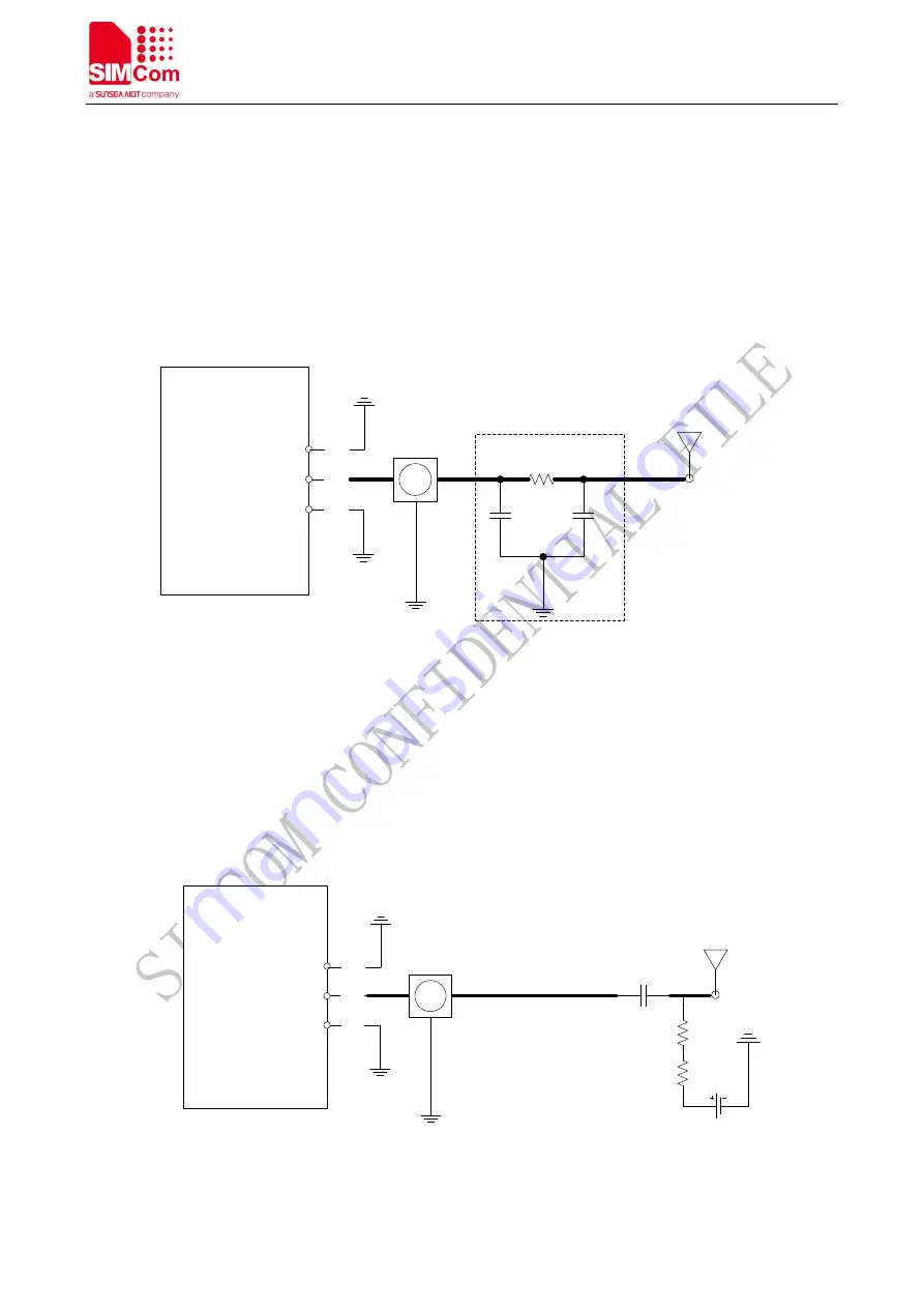
Figure 36: MAIN antenna recommended circuit
R1, C1 and C2 are antenna matching components in Figure 36, the value of these components are determined
according to the antenna tuning results. By default, R1 is 0Ω, C1 and C2 are reserved. The RF connector in Figure
36 is used to ensure the accuracy and convenience of the conduction testing, so SIMCOM suggest keeping it. If
considering Low-Cost BOM, user can cancel the connector.
4.19.2
GNSS Antenna reference circuit
The recommended circuit is shown as
RF connector
(optional)
C1
Module
121
ANT_GNSS
GND
C2
122
R1
Matching circuit
GNSS Passive
ANT
120
GND
Figure 37: GNSSantenna recommended circuit
R1, C1 and C2 are antenna matching components in Figure 37, the value of these components are determined
according to the antenna tuning results. By default, R1 is 0Ω, C1 and C2 are reserved. The RF connector in Figure
37 is used to ensure the accuracy and convenience of the conduction testing, so SIMCOM suggest keeping it. If
considering Low-Cost BOM, user can cancel the connector.
The module has internal LAN, so there is no need for external active antenna. But if the antenna is far away the
module and need a long cable to connect, users can use external active antenna, the recommended circuit is shown
Figure 38:
RF connector
(optional)
Module
121
ANT_GNSS
GND
122
GNSS Active ANT
120
GND
VDD
47nH
10ohm
C1
Figure 38: GNSS active antenna circuit
In Figure 38, the VDD is used to provide voltage to the external active antenna and its value should be taken