background image

Table 22. 

CN8 Ethernet connector pinout

Pin

Pin name

Function

1

TX1+

First bidirectional pair to transmit and receive data.

2

TX1-

3

TX2+

Second bidirectional pair to transmit and receive data.

4

TX2-

5

CT1

Common connected to GND.

6

CT2

Common connected to GND.

7

TX3+

Third bidirectional pair to transmit and receive data.

8

TX3-

9

TX4+

Fourth bidirectional pair to transmit and receive data.

10

TX4-

11

GA

Green LED anode.

12

GC

Green LED cathode.

13

YA

Yellow LED anode.

14

YC

Yellow LED cathode.

15

GND

GND.

16

GND

GND.

6.16

ARDUINO

®

 connectors

6.16.1

Description

The ARDUINO

®

 Uno V3 connectors (CN13, CN14, CN16, and CN17) are available on the STM32MP157x-DKx

Discovery kit. Most shields designed for ARDUINO

®

 can fit with the Discovery kit to offer flexibility in small form

factor applications.

6.16.2

Operating voltage

The ARDUINO

®

 Uno V3 connectors support 5 V, 3.3 V, and VDD for I/O compatibility.

Caution:

Do not supply 3.3 V or 5 V from the ARDUINO

®

 shield. Supplying 3.3 V or 5 V from the ARDUINO

®

 shield could

damage the Discovery kit.

UM2637

ARDUINO® connectors

UM2637

 - 

Rev 2

page 26/47

Содержание STM32MP157 Series

Страница 1: ...ended GPIOs ARDUINO Wi Fi 802 11b g n Bluetooth Low Energy 4 1 and ST LINK V2 1 UART console The STM32MP157F DK2 shown with display removed in Figure 1 and Figure 2 is used as a reference design for user application development It cannot be considered as the hardware design of a final application The hardware features of the Discovery kits are available for users to develop their applications USB ...

Страница 2: ...Raspberry Pi shield capability ARDUINO Uno V3 expansion connectors On board ST LINK V2 1 debugger programmer with USB re enumeration capability Virtual COM port and debug port STM32CubeMP1 and full mainline open source Linux STM32 MPU OpenSTLinux Distribution such as STM32MP1Starter software and examples Support of a wide choice of Integrated Development Environments IDEs including IAR Embedded Wo...

Страница 3: ...1 LCD extension board 2 1 Codification The meaning of the codification is explained in Table 2 Table 2 Codification explanation STM32MP1XXY DKZ Description Example STM32MP157F DK2 STM32MP1 MPU series in STM32 Arm Cortex MPUs STM32MP1 Series XX MPU product line in the series STM32MP157 Y Options D basic security 800 MHz increased frequency F Secure Boot cryptography hardware 800 MHz increased frequ...

Страница 4: ...trademarks are the property of their respective owners 3 2 Development toolchains IAR Systems IAR Embedded Workbench 1 Keil MDK ARM 1 STMicroelectronics STM32CubeIDE GCC 1 On Windows only 3 3 Demonstration software The STM32 MPU OpenSTLinux Distribution and STM32CubeMP1 base demonstration software is preloaded in the microSD for easy demonstration of the device peripherals in standalone mode The l...

Страница 5: ...Jumper JPx OFF Jumper not fitted Jumper JPx 1 2 Jumper fitted between Pin 1 and Pin 2 Solder bridge SBx ON SBx connections closed by 0 Ω resistor Solder bridge SBx OFF SBx connections left open Resistor Rx ON Resistor soldered Resistor Rx OFF Resistor not soldered Capacitor Cx ON Capacitor soldered Capacitor Cx OFF Capacitor not soldered UM2637 Conventions UM2637 Rev 2 page 5 47 ...

Страница 6: ...st use check the board for any damage that might have occurred during shipment that all socketed components are firmly fixed in their sockets and that none are loose in the plastic bag UM2637 Delivery recommendations UM2637 Rev 2 page 6 47 ...

Страница 7: ...tooth Low Energy V4 1 UART microSD card connector SDMMC HSI I2C1 GPIO User interface 4x LEDs User interface RESET buttons GPIO SAI Audio DAC amplifier Stereo jack line out Mic_IN STPMIC1 5V_VIN Type C Type C cable 24 MHz crystal I2C1 I2C1 GPIO 40 pin connector GPIOs Wi Fi 802 11 b g n SDMMC DDR3L DDR LTDC HDMI RGMII Ethernet DSI I2C4 I2C4 I2C1 I2C4 Power supply Feature not available on STM32MP157D...

Страница 8: ... STPMIC U4 40 pin connector CN2 USB Hub U7 DDR3L U5 USB Host CN1 HDMI bridge U14 STM32MP157 U13 USB Host CN5 USB Type C CN7 HDMI CN9 STUSB1600 U12 Wake up button B1 Reset button B2 User1 button B3 User2 button B4 Audio connector CN10 User LED LD5 User LED LD6 User LEDs LD7 LD8 STLK LED LD4 ST LINK USB CN11 ST LINK STM32 U19 UM2637 Hardware layout and configuration UM2637 Rev 2 page 8 47 ...

Страница 9: ...57x DKx Discovery kit The embedded ST LINK V2 1 supports only SWD and VCP for STM32 devices For information about the debugging and programming features of ST LINK V2 1 refer to the ST LINK V2 in circuit debugger programmer for STM8 and STM32 user manual UM1075 and Overview of ST LINK derivatives technical note TN1235 It is recommended to power the board 5V_VIN before plugging the USB debug cable ...

Страница 10: ...tay up to date with the latest firmware version 6 2 Power supply 6 2 1 5 V power supply The STM32MP157x DKx Discovery kit is designed to be powered by a 5 V DC power source at 3 A maximum such as 5V_VBUS connected to the CN6 connector through a USB Type C to USB Type C cable The two lines USB_PWR_CC1 and USB_PWR_CC2 are connected to PA4 and PA5 respectively to check what is connected to CN6 and co...

Страница 11: ... clock references The HSE clock references on the STM32MP157x microprocessor are provided by the external crystal X6 24 MHz crystal from NDK reference NX2016SA 6 4 Reset sources The reset signal of STM32MP157x DKx is active low The internal PU forces the RST signal to a high level The sources of reset are Reset button B2 black button STPMIC1 Embedded ST LINK V2 1 ARDUINO connector CN16 pin 3 reset...

Страница 12: ...UDIO dedicated 1 8 V source provided by the STPMIC1 6 6 3 Audio codec interface Audio codec interfacing is performed through the SAI2 and I2C1 interfaces of the STM32MP157x Table 6 describes the I O configuration of the audio codec interface Table 6 I O configuration for the audio interface I O Configuration PG9 PG9 used as AUDIO RESETN active LOW PE0 PE0 used as SAI2_MCLKA PF11 PF11 used as SAI2_...

Страница 13: ...ted to GND gives the least significant address bit The address of the audio codec is 0b1001010x 0x94 to write and 0x95 to read 6 6 5 Audio jack connector Figure 8 shows the CN10 audio jack connector pinout Figure 8 CN10 audio jack connector pinout Table 7 describes the CN10 audio jack connector pinout Table 7 CN10 audio jack connector pinout Pin Pin name Signal name Codec pin Function 1 1 MIC_IN M...

Страница 14: ...O Configuration PD12 PD12 used as I2C1_SCL shared between AUDIO DSI and HDMI 1 PF15 PF15 used as I2C1_SDA shared between AUDIO DSI and HDMI 1 USB_DP1 USB1_P USB_DM1 USB1_N 1 I2C1 not connected by default SB7 and SB8 OFF Figure 9 shows the CN1 and CN5 USB Type A connector pinout Figure 9 CN1 and CN5 USB Type A connector pinout Table 9 describes CN1 and CN5 USB Host connector pinout Table 9 CN1 and ...

Страница 15: ...pe C Source mode 6 8 2 Operating voltage The STM32MP157D DK1 and STM32MP157F DK2 Discovery kits support 5 V USB voltage from 4 75 V to 5 25 V 6 8 3 USB HS Source When a USB Device connection to the CN7 USB Type C connector of STM32MP157D DK1 or STM32MP157F DK2 is detected the Discovery kit starts behaving as a USB Host 6 8 4 USB Type C connector Figure 10 shows the pinout of USB Type C connector C...

Страница 16: ...tage The microSD card interface is only compatible with the 3 3 V voltage range from 2 7 V to 3 6 V All microSD card types are supported including SDHC and SDXC but only Default and High Speed modes 3 V are supported on STM32MP157D DK1 and STM32MP157F DK2 UHS I modes 1 8 V are not supported on these Discovery kits 6 9 3 microSD card interface The microSD card interface is used in the four data lin...

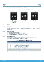
Страница 17: ...0 SDMMC1_D0 PC8 SDIO D0 8 DAT1 SDMMC1_D1 PC9 SDIO D1 9 GND GND GND 10 CARD_DETECT uSD_DETECT PB7 SDCARD_DETECT active LOW 6 10 LEDs 6 10 1 Description The LD2 LED turns green when the power cable is inserted in connector CN6 Two general purpose color LEDs LD7 and LD8 are available as light indicators The LD7 orange LED is used as STM32Cube examples verdict LED The LD8 blue LED is used as Linux Hea...

Страница 18: ...w power mode Connected to STPMIC1 PONKEY which generates a wake up signal on STM32MP157x PA0 Reset button B2 Used to reset the Discovery kit USER1 button B3 Used at boot time by U Boot to enter the USB programming mode USER2 button B4 Used at boot time by U Boot to enter the Android Fastboot mode 6 11 2 I O interface Table 14 describes the I O configuration for the physical user interface Table 14...

Страница 19: ...B8 PB8 is connected to LTDC_B6 PD8 PD8 is connected to LTDC_B7 PE5 PE5 is connected to LTDC_G0 PE6 PE6 is connected to LTDC_G1 PH13 PH13 is connected to LTDC_G2 PH14 PH14 is connected to LTDC_G3 PH15 PH15 is connected to LTDC_G4 PI0 PI0 is connected to LTDC_G5 PI1 PI1 is connected to LTDC_G6 PI2 PI2 is connected to LTDC_G7 PH2 PH2 is connected to LTDC_R0 PH3 PH3 is connected to LTDC_R1 PH8 PH8 is ...

Страница 20: ...tor CN9 Figure 12 CN9 HDMI connector pinout Table 16 describes the pinout of HDMI connector CN9 Table 16 CN9 HDMI connector pinout Pin Pin name Signal name 1 RX2 TX2C_P 2 GND GND 3 RX2 TX2C_N 4 TX1 TX1C_P 5 GND GND 6 RX1 TX1C_N 7 RX0 TX0C_P 8 GND GND 9 RX0 TX0C_N 10 RXC TXCC_P 11 GND GND 12 RXC TXCC_N 13 CEC CEC_A 14 15 SCL DSCL 16 SDA DSDA 17 GND GND UM2637 HDMI UM2637 Rev 2 page 20 47 ...

Страница 21: ...d to SDMMC2_D3 PB3 PB3 is connected to SDMMC2_D2 PB15 PB15 is connected to SDMMC2_D1 PB14 PB14 is connected to SDMMC2_D0 PG6 PG6 is connected to SDMMC2_CMD PE3 PE3 is connected to SDMMC2_CK PH4 PH4 is connected to WL_REG_ON PD0 PD0 is connected to WL_HOST_WAKE 6 13 4 Bluetooth Low Energy I O interface Table 18 describes the I O configuration for the Bluetooth Low Energy interface Table 18 I O conf...

Страница 22: ... a 4 LCD which supports a resolution of 480 800 dots in 16 7 M colors RGB The touch sensitive panel drive is performed by a self capacitive controller Figure 13 shows the LCD connection to MB1407 and MB1272 Figure 13 LCD connection to MB1407 DSISM connector CN4 MB1407 board CTP connector CN1 DSISM connector CN2 LCD module 6 14 2 Operating voltage The LCD module power supply is connected to VDD_3V3...

Страница 23: ...SI data Lane 0 negative DSI_CKP DSI_CKP is used as clock Lane positive DSI_DKN DSI_DKN is used as clock Lane negative PF2 PF2 is used LCD interrupt lane PA15 PA15 is used as DSI backlight control 1 PD12 PD12 used as I2C1_SCL for the touch panel shared between USB AUDIO HDMI PF15 PF15 used as I2C1_SDA for the touch panel shared between USB AUDIO and HDMI 1 Not used In the default configuration back...

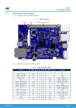
Страница 24: ...ry kits provide a reduced gigabit media independent interface RGMII The STM32MP157x requires an external physical interface device PHY The Ethernet PHY on the Discovery kits is connected to the physical LAN bus using 13 signals for RGMII It can be clocked using the 25 MHz from the STM32MP157x or from a crystal X2 The default configuration is 25 MHz from the X2 crystal The LED LD3 blinks to indicat...

Страница 25: ... as ETH_RXD0 PC5 PB11 is used as ETH_RXD1 PB0 PB0 is used as ETH_RXD2 PB1 PB1 is used as ETH_RXD3 PB11 PB11 is used as ETH_TX_EN PG13 PG13 is used as ETH_TXD0 PG14 PG14 is used as ETH_TXD1 PC2 PB11 is used as ETH_TXD2 PE2 PE2 is used as ETH_TXD3 PA1 PA1 is used as ETH_RX_CLK PG4 PG4 is used as ETH_GTX_CLK PG5 PG5 is used as ETH_CLK125 PB5 PB5 is used as ETH_CLK not the default configuration Figure...

Страница 26: ...ode 13 YA Yellow LED anode 14 YC Yellow LED cathode 15 GND GND 16 GND GND 6 16 ARDUINO connectors 6 16 1 Description The ARDUINO Uno V3 connectors CN13 CN14 CN16 and CN17 are available on the STM32MP157x DKx Discovery kit Most shields designed for ARDUINO can fit with the Discovery kit to offer flexibility in small form factor applications 6 16 2 Operating voltage The ARDUINO Uno V3 connectors sup...

Страница 27: ...Table 23 I O configuration of the ARDUINO interface I O HW Configuration PF14 PF14 is used as ARD_A0 ADC1_IN0 PF13 PF13 is used as ARD_A1 ADC1_IN1 ANA0 ANA0 is used as ARD_A2 ADC1_IN6 ANA1 ANA1 is used as ARD_A3 ADC1_IN2 PC3 SB24 ON PC3 is used as ARD_A4 ADC1_IN13 Default configuration PF12 SB26 ON PF12 is used as ARD_A5 ADC1_IN14 Default configuration PE7 PE7 is used as ARD_D0 UART7_RX PE8 PE8 is...

Страница 28: ...h ARD_A4 SB23 ON SB24 OFF PA11 PA11 used as ARD_D15 I2C5_SCL shared with ARD_A5 SB25 ON SB26 OFF Table 24 describes the pinout of the ARDUINO connectors Table 24 Pinout of the ARDUINO connectors Connector Pin name Signal name STM32 pin Comment CN16 1 NC NC reserved for test 2 3V3 IOREF 3V3 3 NRST NRST NRST 4 3V3 3V3 5 5V 5V 6 GND GND 7 GND GND 8 VIN Not connected CN17 1 A0 PF14 ADC1_IN0 2 A1 PF13 ...

Страница 29: ...DA 10 ARD_D15 PA11 I2C5_SCL 6 17 GPIO expansion connectors 6 17 1 Description The GPIO pins can be used as GPIOs or alternate functions The available alternate functions are listed in Table 25 GPIO connectors pinout Other functions such as I2C UART or FDCAN can be mapped on the GPIO connectors for instance using the STM32CubeMX tool The GPIO expansion connector CN2 offers Raspberry Pi shields capa...

Страница 30: ...2C5_SDA PA12 3 4 5V GPIO3 I2C5_SCL PA11 5 6 GND GPIO4 MCO1 PA8 7 8 PB10 GPIO14 USART3_TX GND 9 10 PB12 GPIO15 USART3_RX GPIO17 USART3_RTS PG8 11 12 PI5 GPIO18 SAI2_SCKA GPIO27 SDMMC3_D3 PD7 13 14 GND GPIO22 SDMMC3_CK PG15 15 16 PF1 GPIO23 SDMMC3_CMD 3V3 17 18 PF0 GPIO24 SDMMC3_D0 GPIO10 SPI5_MOSI PF9 19 20 GND GPIO9 SPI5_MISO PF8 21 22 PF4 GPIO25 SDMMC3_D1 GPIO11 SPI5_SCK PF7 23 24 PF6 GPIO8 SPI5_...

Страница 31: ...3_D2 PF5 37 38 PI6 GPIO20 SAI2_SDA GND 39 40 PF11 GPIO21 SAI2_SDB 6 18 VBAT connector 6 18 1 Description The voltage on the VBAT pin of the STM32MP157x DKx can be provided by an external battery Use connector CN3 to plug a CR2032 battery 3 V lithium battery wired on Molex 51021 0200 as shown in Figure 18 Caution Pin1 VBAT Pin2 GND Figure 18 CN3 VBAT connector 1 2 UM2637 VBAT connector UM2637 Rev 2...

Страница 32: ...the board Some boards feature a specific STM32 device version which allows the operation of any bundled commercial stack library available This STM32 device shows a U marking option at the end of the standard part number and is not available for sales In order to use the same commercial stack in his application a developer may need to purchase a part number specific to this stack library The price...

Страница 33: ...d MB1407 revision C 01 The revision C 01 is the initial release of the display board MB1407 Board limitations No limitation identified for this board revision UM2637 Board revision history UM2637 Rev 2 page 33 47 ...

Страница 34: ...G4 PZ3 BT_PCM_1_WS H4 PI9 LTDC_VSYNC G3 PZ0 BT_PCM_1_CK J4 PZ2 BT_PCM_1_SDO G2 PZ4 PMIC_I2C4_SCL K4 PG12 LTDC_B1 H2 PZ5 PMIC_I2C4_SDA H1 PZ6 BT_REG_ON J3 PZ7 BT_DEV_WAKE D2 PD6 BT_USART2_RX L3 PD14 ARDUINO_D3_TIM4_CH3 J2 PD15 ARDUINO_D5_TIM4_CH4 K3 PD8 LTDC_B7 K1 PD9 LTDC_B0 L4 PI8 LPO_32OUT2 K2 PC13 PC13_ANTI_TAMP_PMIC_WAKEUP N2 PA13 LED1_GPIO T2 PA14 LED2_GPIO P4 PI11 PI11_STUSB1600_IRQN_WKUP5 T...

Страница 35: ... PA2 ETH_MDIO AA6 PC1 ETH_MDC Y6 PG5 ETH_CLK125 AA3 PH3 LTDC_R1 AB6 PB0 ETH_RXD2 Y4 PF15 I2C1_SDA AA7 PB1 ETH_RXD3 AC4 PF14 ARDUINO_A2_ADC2_IN6 Y5 PF13 ARDUINO_A3_ADC2_IN2 AB4 PH2 LTDC_R0 AB7 PC5 ETH_RXD1 AC7 PC4 ETH_RXD0 Y9 PF12 ARDUINO_A5_ADC1_IN6 Y10 PF11 SAI2_SD_B AB8 PA7 ETH_RXDV AC8 PA6 ETH_MDINT AB5 PC0 LTDC_R5 Y3 PB10 GPIO14_USART3_TX AC5 PB12 GPIO15_USART3_RX AA10 PB13 GPIO16_USART3_CTS_N...

Страница 36: ...PIO3_I2C5_SDA AA18 PA11 ARDUINO_D15__GPIO2_I2C5_SCL D16 PC11 uSD_SDMMC1_D3 D19 PE4 DSI_RESET_GPIO D18 PC8 uSD_SDMMC1_D0 D15 PC10 uSD_SDMMC1_D2 B13 PB4 WLAN_SDMMC2_D3 D17 PC9 uSD_SDMMC1_D1 B11 PC7 GPIO13_TIM3_CH2 B14 PC6 DSI_TE A14 PF2 DSI_LCD_INT_GPIO D12 PD2 uSD_SDMMC1_CMD A13 PA8 GPIO4_MCO1 C13 PB14 WLAN_SDMMC2_D0 D13 PC12 uSD_SDMMC1_CK B12 PB15 WLAN_SDMMC2_D1 C11 PE5 LTDC_G0 A11 PB3 WLAN_SDMMC2...

Страница 37: ...3_CMD D9 PF4 GPIO25_SDMMC3_D1 B6 PD4 BT_USART2_RTS D7 PF5 GPIO26_SDMMC3_D2 B5 PD10 LTDC_B3 D6 PE0 SAI2_MCLK_A C8 PE1 ARDUINO_D2_GPIO D5 PH8 LTDC_R2 C5 PH9 LTDC_R3 A4 PE11 ARDUINO_D10_SPI4_NSS TIM1_CH2 B4 PE12 ARDUINO_D13_SPI4_SCK A3 PE13 ARDUINO_D12_SPI4_MISO C4 PH11 GPIO6_TIM5_CH2 C6 PE14 ARDUINO_D11_SPI4_MOSI TIM1_CH4 D3 PE15 LTDC_R7 B3 PH4 WLAN_REG_ON_GPIO UM2637 STM32MP157x DKx I O assignment ...

Страница 38: ...ense Note Use only shielded cables for USB Ethernet HDMI cables Use added ferrite clamp on audio cable one turn Responsible party in the USA Terry Blanchard Americas Region Legal Group Vice President and Regional Legal Counsel The Americas STMicroelectronics Inc 750 Canyon Drive Suite 300 Coppell Texas 75019 USA ISED Canada ICES 003 CAN ICES 3 A NMB 3 A 9 1 Additional FCC and ISED Canada Complianc...

Страница 39: ...unction with any other antenna or transmitter Pour satisfaire aux exigences FCC et ISDE Canada concernant l exposition aux champs RF pour les appareils mobile une distance de séparation de 20 cm ou plus doit être maintenu entre l antenne de ce dispositif et les personnes pendant le fonctionnement Pour assurer la conformité il est déconseillé d utiliser cet équipement à une distance inférieure Cet ...

Страница 40: ...is equipment may cause radio interference 10 2 Simplified declaration of conformity Hereby STMicroelectronics declares that the radio equipment types STM32MP157D DK1 and STM32MP157F DK2 are in compliance with Directive 2014 53 EU The full text of the EU declaration of conformity is available from their product web page UM2637 CE conformity UM2637 Rev 2 page 40 47 ...

Страница 41: ...assignment in STM32MP157x DKx I O assignment Updated Features Development environment STM32MP157x DKx Discovery kits information and Simplified declaration of conformity Updated figures STM32MP157x DKx hardware block diagram STM32MP157x DKx PCB layout top side and STM32MP157x DKx PCB layout bottom side Removed Technology partners and the component references in Hardware layout and configuration UM...

Страница 42: ...are upgrade 10 6 2 Power supply 10 6 2 1 5 V power supply 10 6 2 2 STPMIC1 power supply 10 6 3 Clock sources 11 6 3 1 LSE clock references 11 6 3 2 HSE clock references 11 6 4 Reset sources 11 6 5 Boot mode 11 6 5 1 Description 11 6 6 Audio 12 6 6 1 Description 12 6 6 2 Operating voltage 12 6 6 3 Audio codec interface 12 6 6 4 Headphone outputs 13 6 6 5 Audio jack connector 13 6 6 6 I O restrictio...

Страница 43: ...Fi and Bluetooth Low Energy 21 6 13 1 Description 21 6 13 2 Operating voltage 21 6 13 3 Wi Fi I O interface 21 6 13 4 Bluetooth Low Energy I O interface 21 6 14 MIPI DSISM LCD 22 6 14 1 Description 22 6 14 2 Operating voltage 22 6 14 3 LCD interface 23 6 15 Gigabit Ethernet 24 6 15 1 Description 24 6 15 2 Operating voltage 24 6 15 3 Ethernet interface 25 6 16 ARDUINO connectors 26 6 16 1 Descripti...

Страница 44: ... AU1 32 7 4 Board revision history 32 7 4 1 Board MB1272 revision C 02 32 7 4 2 Board MB1407 revision C 01 33 8 STM32MP157x DKx I O assignment 34 9 Federal Communications Commission FCC and ISED Canada Compliance Statements 38 9 1 Additional FCC and ISED Canada Compliance Statements for STM32MP157F DK2 38 10 CE conformity 40 10 1 Warning 40 10 2 Simplified declaration of conformity 40 Revision his...

Страница 45: ...the LED interfaces 18 Table 14 I O configuration for the physical user interface 18 Table 15 I O configuration for the HDMI interface 19 Table 16 CN9 HDMI connector pinout 20 Table 17 I O configuration for the Wi Fi interface 21 Table 18 I O configuration for the Bluetooth Low Energy interface 21 Table 19 I O configuration of the LCD and CTP interfaces 23 Table 20 LCD interface and CN4 connector p...

Страница 46: ...mode switch SW1 12 Figure 8 CN10 audio jack connector pinout 13 Figure 9 CN1 and CN5 USB Type A connector pinout 14 Figure 10 CN7 USB Type C connector pinout 15 Figure 11 microSD card connector CN15 17 Figure 12 CN9 HDMI connector pinout 20 Figure 13 LCD connection to MB1407 22 Figure 14 CN4 LCD connector pinout 23 Figure 15 CN8 Ethernet connector pinout 25 Figure 16 ARDUINO connectors pinout 27 F...

Страница 47: ...cts and ST assumes no liability for application assistance or the design of Purchasers products No license express or implied to any intellectual property right is granted by ST herein Resale of ST products with provisions different from the information set forth herein shall void any warranty granted by ST for such product ST and the ST logo are trademarks of ST For additional information about S...

Отзывы: