


Running the IBU UI tool
UM0935
22/53
Doc ID 17398 Rev 3
3.3.1
Steps for making hardware connection
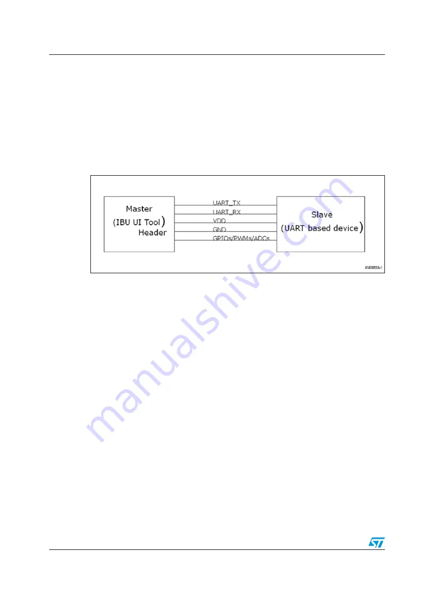
To use any UART (SCI) based slave with the IBU UI tool, you need to make the connection
for jumper J1, as shown in
●
The TX (transmitter), RX (receiver), and GND (ground line) should be connected to the
corresponding lines of the daughter board for UART (SCI) communication
●
VDD equal to 3.3 V (power supply line) of the two boards should be connected if the
daughter board is to be powered using the IBU UI tool
●
The GPIOs of the IBU UI tool and daughter board can be connected or left
unconnected as per user requirements.
Figure 16.
Connection diagram for the 10-pin UART interface/GPIOs
3.3.2 GPIO
settings
For the GPIO which is to be used along with the UART (SCI) interface, it is necessary to
make the proper settings. These GPIOs may be used as control lines, chip select or status
line, such as interrupt line, or to generate a clock signal using the PWM feature available on
two pins, therefore, you need to make the GPIOs settings accordingly.
To understand the modes that are supported by a particular pin, please refer to
.
By default UART_GPIO1 to UART_GPIO4 are in input pull-up mode.
Here you can set only the GPIOs mentioned. UART (TX, RX, CTS, and RTS) lines and
power lines are fixed. To perform the settings of a GPIO, use the UART (SCI) DLL referring
to the DLL help file available.
Through selection, the GPIO can be set in different modes, such as simple input mode,
input with interrupt, and push pull output mode. Also in the UART (SCI) interface, there is an
option in GPIO3 and GPIO4 to use this GPIO as the PWM clock signal and there is an
option in GPIO4 to use it as an ADC channel.
3.3.3 Using
GPIOs in PWM settings
As mentioned above, GPIO 3 and GPIO 4 can also additionally be set in PWM mode. To do
this, set the GPIO3 or GPIO4 in PWM mode and provide the PWM frequency (maximum
value tested is around 10 MHz) and also the duty cycle to generate different kinds of clocks.
The frequency of the PWM clock generated can vary from 10 kHz to 10MHz. The duty cycle
of the PWM clock can vary from 0 % to 100 %. Logic '0' is obtained with the duty cycle at 0
% and logic '1' is obtained with the duty cycle at 100 %. Please refer to
.
10-pin
Содержание STEVAL-PCC009V2
Страница 4: ...Contents UM0935 4 53 Doc ID 17398 Rev 3 Appendix D Tables and figures 50 Revision history 52...
Страница 42: ...UM0935 Schematics and BOM list Doc ID 17398 Rev 3 42 53 Figure 32 10 pin com interface V...
Страница 43: ...Schematics and BOM list UM0935 43 53 Doc ID 17398 Rev 3 Figure 33 30 pin com interface V...


