


UM0529
Pin assignments
17/29
Thus it can be seen by comparing
column 3 (input 1A) and column 4 (output Y0), that the
CON signal is getting buffered. Hence only the voltage level conversion from 5 V to 3.3 V is
done.
Note:
Second input of U3 is not used in the application. However, to save the current consumption,
these inputs are not left floating and are tied to ground.
5.6
STUSB02E and STUSB03 transceiver pin configuration
shows the pin description of STUSB02E transceiver.
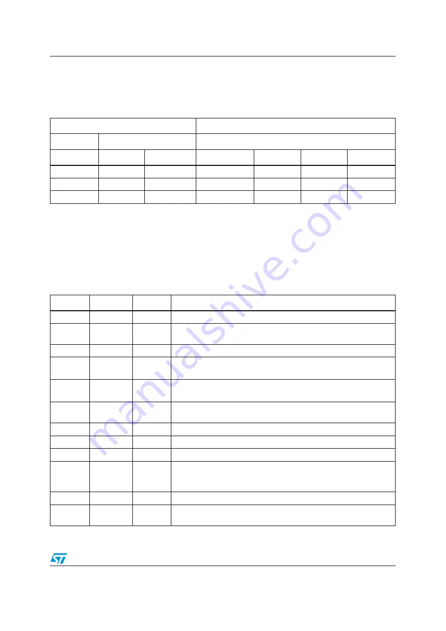
Table 13.
Truth table for second input of U3
Inputs
Outputs
Enable
Select
n2G(15)=VCC 2B(13)=GND
2A(14) = GND
nY0(12) =NC
nY1(11)= NC nY2(10) = NC
nY3(9) = NC
H
x
X
H
H
H
H
L
L
L
L
H
H
H
L
L
H
H
L
H
H
Table 14.
Pin description for STUSB02E transceiver
Pin no.
Symbol
I/O
Name and function
0
N.C
Not connected
1
SPD
I
Edge rate control. A logic HIGH operates at edge rates for “full-speed”
operation. A logic LOW operates edge rates for “low-speed” operation.
2
RCV
O
Receive data. Output for USB differential data.
3
VP
I/O
If OE# = H, VP = receiver output (+)
If OE# = L, VP = driver input (+)
4
VM
I/O
If OE# = H, VM = receiver output (-)
If OE# = L, VM = driver input (-)
5
CON
I
CONNECT (input). Controls state of VPU. Refer to VPU pin description for
details.
6
GND
Ground reference
7
SUS
I
Suspend (active-high). Turns off internal circuits to reduce supply current.
8
N.C.
Not connected
9
OE#
I
Output enable (active-low). Enables transceiver data transmission to the
bus.
When not active, the transceiver is in the receive mode.
10, 11
D-, D+
I/O
Differential data lines.
12
VTRM
O
3.3 V reference supply output. Requires a 1.0
µ
F decoupling capacitor for
stability.
www.BDTIC.com/ST