


Pin mapping
AN4159
8/27
Doc ID 023639 Rev 3
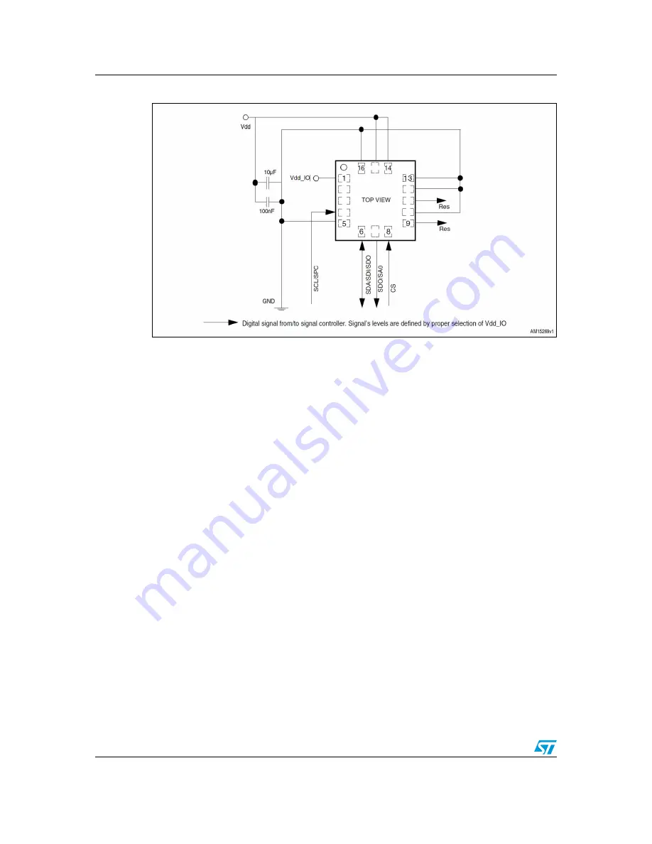
Figure 5.
LPS331AP electrical connection
Key notes:
●
SDA and SCL pull-up resistors should be connected to VDD_IO
●
VDD_IO should be same or lower than VDD (use level shifters otherwise)
●
If VDD_IO is higher than VDD, high non-destructive current may occur
●
If there is choice and interface is I2C, use SA0 = VDDIO slave address by default.
3.0.1
Pressure sensor PCB layout and solder recommendations
The LPS331AP has an opening on top of the package, sensor performance can be
compromised by:
●
Mechanical stress coming from PCB board
–
The whole package s air should have minimum temperature gradient
–
Avoid placement in long and narrow PCB area, warp free area
●
Temperature gradients (non-uniform/rapidly changing temperature around sensor)
●
Strong electrical field / light source
●
Localized air pressure stability (unwanted fast air pressure variation, fans)
●
Dust and water exposure/condensation (GORE-TEX
®
protection, etc.)


