Wireless Module
All Rights Reserved. SparkLAN may make changes to specification and descriptions at any time without prior notice.
www.sparklan.com / [email protected] / +886 2 2659-1880
WPEQ-405AX
Ver.0.94
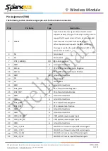
Pin Assignment (TBD)
The following section illustrate signal pin-outs for the module connector.
TOP
Pin#
Pin Name
Type
Description
1
WAKE#
-
Open Drain active Low signal. When the add-in card
supports wakeup, this signal is used by the add-in card to
request that the system return from a sleep/suspended
state to service a function initiated wake event.
When the add-in card supports the OBFF mechanism,
this signal is used by the system to indicate OBFF or CPU
Active State transitions.
3
NC
-
No connect
5
NC
-
No connect
7
PCIE_CLKREQ_L
OD PCIe clock request
9
GND
G
Ground connections
11
REFCLK-
I
PCIe differential clock input- Negative
13
I
PCIe differential clock input- Positive
15
GND
G
Ground connections
17
NC
-
No connect
19
NC
-
No connect
21
GND
G
Ground connections
23
PCIE_TDN
O
PCIe Transmit data-Negative
25
PCIE_TDP
O
PCIe Transmit data-Positive
27
GND
G
Ground connections
29
GND
G
Ground connections
31
PCIE_RDN
I
PCIe receive data-Negative
33
PCIE_RDP
I
PCIe receive data-Positive
35
GND
G
Ground connections
37
GND
G
Ground connections
39
VDD_3V3_SIP
P
VDD system power supply input
41
VDD_3V3_SIP
P
VDD system power supply input
43
GND
G
Ground connections
45
PCIE_L1_TXM
-
WLAN PCIe L1 transmit output differential signals
47
PCIE_L1_TXP
-
WLAN PCIe L1 transmit output differential signals
49
PCIE_L1_RXM
-
WLAN PCIe L1 receive input differential signals
51
PCIE_L1_RXP
-
WLAN PCIe L1 receive input differential signals


