


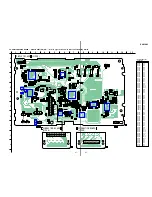


19
19
XVM-H65
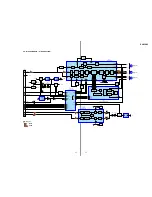
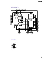
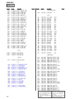
• Waveforms (DISPLAY Board)
1
TP505
1V/DIV 50µsec/DIV
127µsec
2
0.2V/DIV 20µsec/DIV
3
0.2V/DIV 20µsec/DIV
H
0
10V/DIV 5µsec/DIV
14.7µsec
qa
1V/DIV 5msec/DIV
16.4µsec
3.5Vp-p
H
1Vp-p
1Vp-p
30.7Vp-p
3.5Vp-p
4
0.2V/DIV 200nsec/DIV
3.5714MHz
5
0.5V/DIV 200nsec/DIV
6
0.5V/DIV 200nsec/DIV
2.3MHz
qs
1V/DIV 50µsec/DIV
128µsec
qd
1V/DIV 20µsec/DIV
62.6µsec
qf
1V/DIV 50µsec/DIV
190.9µsec
0.8Vp-p
2.8MHz
1.1Vp-p
1.1Vp-p
3.5Vp-p
3.5Vp-p
3.5Vp-p
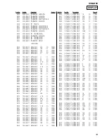
7
1V/DIV 10msec/DIV
16.5µsec
8
1V/DIV 20µsec/DIV
qh
1V/DIV 50nsec/DIV
7.2MHz
qg
1V/DIV 10µsec/DIV
63.4µsec
3.5Vp-p
64µsec
3.6Vp-p
3.6Vp-p
2.8Vp-p
9
5V/DIV 5µsec/DIV
8.4µsec
13.2Vp-p
qk
5V/DIV 2µsec/DIV
4.2µsec
ql
10V/DIV 2µsec/DIV
4.2µsec
11.8Vp-p
35Vp-p
w;
0.5V/DIV 20µsec/DIV
63µsec
wa
2V/DIV 50µsec/DIV
127µsec
ws
1V/DIV 20µsec/DIV
2H
2.2Vp-p
4.4Vp-p
3.3Vp-p
wf
1V/DIV 20µsec/DIV
2H
wd
1V/DIV 20µsec/DIV
2H
3.3Vp-p
3.2Vp-p
qj
0.2V/DIV 50nsec/DIV
14.48MHz
5.4Vp-p
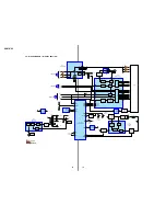
TP506
TP507
TP508
TP352
TP353
TP406
TP407
TP850
TP851
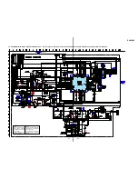
TP601
TP602
TP603
TP606
TP609
TP611
TP612
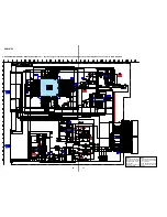
TP801
TP802
TP808
TP809
TP810
TP811
TP812
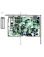
THIS NOTE IS COMMON FOR PRINTED WIRING
BOARDS AND SCHEMATIC DIAGRAMS.
(In addition to this, the necessary note is
printed in each block.)
for schematic diagram:
• All capacitors are in µF unless otherwise noted. pF: µµF
50 WV or less are not indicated except for electrolytics
and tantalums.
• All resistors are in
Ω
and
1
/
4
W or less unless otherwise
specified.
•
%
: indicates tolerance.
•
f
: internal component.
•
C
: panel designation.
Caution:
Pattern face side: Parts on the pattern face side seen from the
(Side B)
pattern face are indicated.
Parts face side: Parts on the parts face side seen from the
(Side A)
parts face are indicated.
•
A
: B+ Line.
•
B
: B– Line.
•
H
: adjustment for repair.
• CN401 of XVM-H65D is connected to Connection Box
with a monitor cable.
Power voltage is dc 14.4 V from ACC cord of the Connec-
tion Box and fed with regulated dc power supply.
• CN401 of XVM-H65D is connected to Connection Box
with a monitor cable.
Voltage and waveforms are measured at input the color
bar signal from the Connection Box.
• Voltages are taken with a VOM (Input impedance 10 M
Ω
).
Voltage variations may be noted due to normal produc-
tion tolerances.
• Waveforms are taken with a oscilloscope.
Voltage variations may be noted due to normal produc-
tion tolerances.
• Circled numbers refer to waveforms.
• Signal path.
F
: AUDIO
g
: VIDEO
for printed wiring boards:
•
X
: parts extracted from the component side.
•
Y
: parts extracted from the conductor side.
•
: Pattern from the side which enables seeing.
Note:
The components identi-
fied by mark
0
or dotted
line with mark
0
are criti-
cal for safety.
Replace only with part
number specified.
Note:
Les composants identifiés par
une marque
0
sont critiques
pour la sécurité.
Ne les remplacer que par une
piéce por tant le numéro
spécifié.


