


– 6 –
SECTION 3
DIAGRAMS
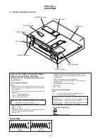
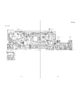
3-1. CIRCUIT BOARDS LOCATION
THIS NOTE IS COMMON FOR PRINTED WIRING
BOARDS AND SCHEMATIC DIAGRAMS.
(In addition to this, the necessary note is printed
in each block.)
For schematic diagrams.
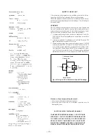
Note:
• All capacitors are in µF unless otherwise noted. pF: µµF
50 WV or less are not indicated except for electrolytics
and tantalums.
• All resistors are in
Ω
and
1
/
4
W or less unless otherwise
specified.
•
¢
: internal component.
•
2
: nonflammable resistor.
•
C
: panel designation.
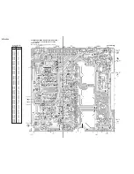
For printed wiring boards.
Note:
•
X
: parts extracted from the component side.
•
b
: Pattern of the conductor side.
•
U
: B+ Line.
•
V
: B– Line.
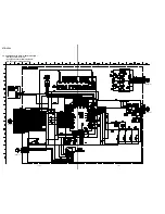
• Voltages and waveforms are dc with respect to ground
under no-signal (detuned) conditions.
no mark : FM
WAVEFORMS
1 2
IC201
#¢
X1
IC300
@¢
Note: The components identified by mark
!
or dotted line
with mark
!
are critical for safety.
Replace only with part number specified.
• Indication of transistor
C
These are omitted
E
B
8MHz
4.8Vp-p
4.19MHz
5.4Vp-p
Caution:
Pattern face side: Parts on the pattern face side seen from
(Conductor Side) the pattern face are indicated.
Parts face side: Parts on the parts face side seen from
(Component Side)
the parts face are indicated.
• Voltages are taken with a VOM (Input impedance 10 M
Ω
).
Voltage variations may be noted due to normal produc-
tion tolerances.
• Waveforms are taken with a oscilloscope.
Voltage variations may be noted due to normal produc-
tion tolerances.
• Circled numbers refer to waveforms.
• Signal path.
F
: FM
SECONDARY board
PRIMARY board
STANDBY board
MAIN board
VOL-TONE board
DISPLAY board
SPEAKER SW board
KEY board
POWER SW board
Содержание STR-V200 - Fm Stereo/fm-am Receiver
Страница 5: ... 5 This section is extracted from instruction manual ...
Страница 13: ... 19 20 STR V200 Component Side ...
Страница 15: ... 23 24 STR V200 Component Side ...
Страница 17: ... 27 28 STR V200 Component Side ...