


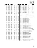


STR-DE185
15
15
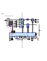
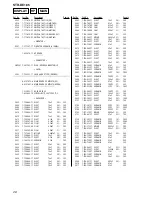
THIS NOTE IS COMMON FOR PRINTED WIRING
BOARDS AND SCHEMATIC DIAGRAMS.
(In addition to this, the necessary note is
printed in each block.)
for schematic diagram:
• All capacitors are in µF unless otherwise noted. pF: µµF
50 WV or less are not indicated except for electrolytics
and tantalums.
• All resistors are in
Ω
and
1
/
4
W or less unless otherwise
specified.
•
f
: internal component.
•
2
: nonflammable resistor.
•
1
: fusible resistor.
•
C
: panel designation.
•
A
: B+ Line.
•
B
: B– Line.
• Voltage and waveforms are dc with respect to ground
under no-signal (detuned) conditions.
no mark : FM
• Voltages are taken with a VOM (Input impedance 10 M
Ω
).
Voltage variations may be noted due to normal produc-
tion tolerances.
• Waveforms are taken with a oscilloscope.
Voltage variations may be noted due to normal produc-
tion tolerances.
• Circled numbers refer to waveforms.
• Signal path.
F
: FM/AM
L
: MD/TAPE
g
: VIDEO 1
J
: CD
c
: VIDEO 2
Note:
The components identified by mark
0
or dotted line
with mark
0
are critical for safety.
Replace only with part number specified.
for printed wiring boards:
•
X
: parts extracted from the component side.
•
f
: internal component.
•
: Pattern from the side which enables seeing.
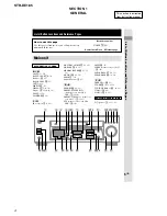
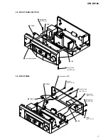
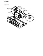
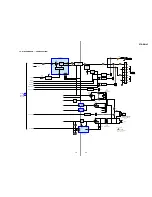
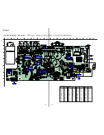
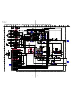
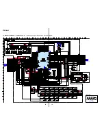
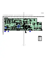
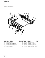
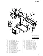
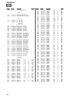
4-6. PRINTED WIRING BOARDS — H/P, OUTLET SECTION — • Refer to page 11 for Circuit Boards Location.
1
A
B
C
D
E
F
G
H
I
J
2
3
4
5
6
7
CNP801
J803
CNJ901
CNP907
(Page 14)
(Page 14)
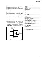
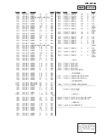
Содержание STR-DE185
Страница 31: ...31 STR DE185 MEMO ...


