


11
STR-DB900
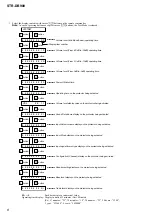
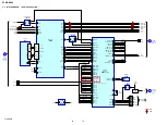
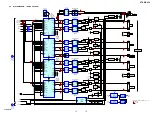
Note on Schematic Diagram:
• All capacitors are in
µ
F unless otherwise noted. (p: pF)
50 WV or less are not indicated except for electrolytics and
tantalums.
• All resistors are in
Ω
and
1
/
4
W or less unless otherwise
specified.
• %
: indicates tolerance.
•
f
: internal component.
•
2
: nonflammable resistor.
•
C
: panel designation.
•
A
: B+ Line.
•
B
: B– Line.
• Voltages and waveforms are dc with respect to ground un-
der no-signal conditions.
No mark : FM
*
: Impossible to measure
• Voltages are taken with a VOM (Input impedance 10 M
Ω
).
Voltage variations may be noted due to normal production
tolerances.
• Waveforms are taken with a oscilloscope.
Voltage variations may be noted due to normal production
tolerances.
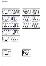
• Circled numbers refer to waveforms.
• Signal path.
F
: FM
g
: VIDEO
• Abbreviation
SP
: Singapore model
MY
: Malaysia model
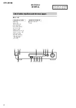
NOTE FOR PRINTED WIRING BOARDS AND SCHEMATIC DIAGRAMS
(In addition to this necessary note is printed in each block.)
Note on Printed Wiring Board:
•
X
: parts extracted from the component side.
•
a
: Through hole.
•
: Pattern from the side which enables seeing.
• Abbreviation
SP
: Singapore model
MY
: Malaysia model
Caution:
Pattern face side: Parts on the parts face side seen from
(Side A)
the parts face are indicated.
Parts face side:
Parts on the pattern face side seen from
(Side B)
the pattern face are indicated.
Note: The components identified by mark
0
or dotted
line with mark
0
are critical for safety.
Replace only with part number specified.
Содержание STR-DB900
Страница 63: ...63 STR DB900 MEMO ...


