


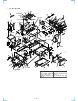


– 68 –
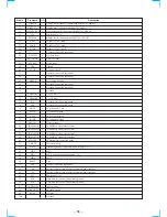
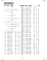
I/O
O
O
I
O
I
—
O
I
I
I
I
—
—
—
I
—
I
O
—
O
O
O
I
—
—
I
O
O
O
O
—
O
O
O
O
O
O
O
O
I
I
I
—
I
I
I
I
—
Description
EIAJ data and parity flag output terminal
Emphasis monitor output terminal ("H" = ON)
RC oscillator input terminal
RC oscillator output terminal
Microprocessor I/F select input terminal (CCB: H, SUB: L) (Connected to ground)
Digital ground
Clock output select terminal ("L" = 256 fs, "H" = 128 fs) (Connected to ground)
Clock input select terminal ("H" = 512 fs, "L" = 384 fs)
Test terminal (Connected to ground)
Test terminal (Connected to ground)
Reset input terminal
Digital power supply 0.5 V
Not used (Not connected, open)
Analog power 5 V
VCO oscillation band adjustment input terminal
Analog ground
VCO free-running frequency setting input terminal
External LPF is connected to this terminal for PLL
Digital power 5 V
CD subcode I/F and block sync output terminal
CD subcode I/F and data output terminal
CD subcode I/F and frame sync output terminal
CD subcode I/F and shift clock input terminal for data reading
Digital ground
Digital power 5 V
Crystal oscillator input terminal
Crystal oscillator output terminal
VCO and crystal oscillator clock output terminal
256fs or 128fs clock output terminal (Selected by CLKMD terminal)
Error mute output terminal
Digital ground
Sampling frequency monitor output terminal
Sampling frequency monitor output terminal
Bit clock output terminal
Audio data output terminal
L, R clock output terminal (L-ch: H, R-ch: L)
Microprocessor I/F and subcode Q data sync output terminal
Microprocessor I/F. When CCB/SUB is L, data output terminal (3-state output)
Microprocessor I/F. When CCB/SUB is H, data output terminal (high level open drain output) (Not connected)
Microprocessor I/F. Data input terminal
Microprocessor I/F. Chip enable/latch input terminal
Microprocessor I/F. Clock input terminal
Digital power 5 V
Built-in amplifier data input terminal (Connected to ground)
Built-in amplifier data input terminal (Connected to ground)
Built-in amplifier data input terminal (Connected to ground)
Built-in amplifier data input terminal
Digital ground
Pin No.
1
2
3
4
5
6
7
8
9
10
11
12
13
14
15
16
17
18
19
20
21
22
23
24
25
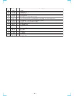
26
27
28
29
30
31
32
33
34
35
36
37
38
39
40
41
42
43
44
45
46
47
48
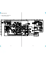
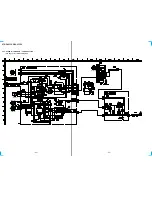
IC1101
CXD8495AQ (DIGITAL BOARD)
Pin Name
DOUT/V
EMPHA
RC1
RC2
CCB/SUB
D. GND
128/256
384/512
TEST
TEST
RESET
D. +5V
—
A. +5V
R
A. GND
VCO IN
VCO
D. +5V
SBSY
PW
SFSY
SB CLK
D. GND
D. +5V
XIN
XOUT
CLK OUT
CLK OUT
ERROR
D. GND
SUB1
SUB2
BCK
DATA OUT
LRCK
LD/DQSY
SRDT
DO
DI/SWDT
CE/XLAT
CL/SCLK
D. +5V
DIN1
DIN2
DIN3
DIN4
D. GND
Содержание STR-DA333ES - Fm Stereo/fm-am Receiver
Страница 2: ... 2 ...
Страница 6: ... 6 SECTION 2 GENERAL This section is extracted from STR DA555ES instruction manual ...
Страница 7: ... 7 ...
Страница 8: ... 8 ...


