


– 45 –
5-15.
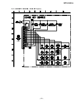
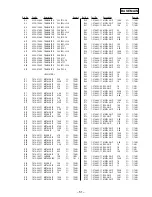
IC PIN FUNCTION DESCRIPTION
•
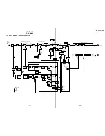
BASE MAIN BOARD IC8 MB89174APF-G-290-BND (SYSTEM CONTROLLER)
Pin No.
Pin Name
I/O
Description
1
DTMF
O
DTMF tone signal output terminal
2
RESET
I
System reset signal input from the reset signal generator (Q15) “L”: reset
For several hundreds msec. after the power supply rises, “L” is input, then it changes to “H”
3, 4
MOD0, MOD1
I
Setting terminal for the CPU operational mode Fixed at “L” in this set
5
X0
I
Main system clock input terminal (3.579545 MHz)
6
X1
O
Main system clock output terminal (3.579545 MHz)
7
VCC
—
Power supply terminal (+5V)
8
X0A
I
Sub system clock input terminal Not used (fixed at “L”)
9
X1A
O
Sub system clock output terminal Not used (open)
10
RLCONT
O
Relay drive signal output terminal “H”: hook on
11
PLL EN
O
Chip enable signal output to the M64884FP (IC302)
When PLL EN goes from “L” to “H”, it load data from PLL DATA
12
PLL DATA
O
PLL serial data output to the M64884FP (IC302)
13
PLL CLK
O
PLL serial data transfer clock signal output to the M64884FP (IC302)
14
TX CNT
O
TX system power supply on/off control signal output “L”: TX system power on
15
MIC MUTE
O
Microphone amplifier on/off control signal output terminal “H”: muting on
16
CHG CONT
O
Charge on/off circuit control signal output terminal
17
TX MUTE
O
Muting control signal output to the IR3N74AN (IC1) “L”: muting on
At TX mode: During sending data to handset, muting it
18
SQ IN
I
Squelch signal (carrier detection signal) input from the MC3361CDR2 (IC3)
“L”: carrier present, “H”: no carrier
19
GND
—
Ground terminal
20
DATA IN
I
Receive data input terminal
21
CHG DET
I
Charge detection signal input terminal “L”: charge on
22
PARADET
I
Establish telephone detect signal input terminal “L”: off hook
23 to 26
COL0 to COL3
I
Key return signal input from the key matrix
27 to 31
ROW0 to ROW4
O
Key send signal output to the key matrix
32
INT LED
O
LED drive signal output of the INTERCOM indicator (D752) “L”: LED on
33
SP LED
O
LED drive signal output of the SPEAKERPHONE indicator (D753) “L”: LED on
34
SP MUTE1
O
Speaker muting control signal output terminal “H”: muting on
35
LINE LED
O
LED drive signal output of the LINE indicator (D754) “L”: LED on
36
RX MUTE
O
Muting control signal output to the IR3N74AN (IC1) “L”: muting on
At RX mode: After receiving premble bits from handset muting it until data sent finished
37
BELL IN
I
Detect signal input of the ringer coming “L”: ringer coming
38
BELL OUT
O
Bell output terminal to the voice speakerphone (IC5)
39
PWR OFF
I
Battery level detect signal input from the RH5VL40CA (IC7) “L”: battery off
40
TONE/PULSE
I
DIAL MODE switch (S1) input terminal “L”: pulse mode, “H”: tone mode
41
BELL HI
I
RINGER switch (S2) input terminal “L”: volume level is high
42
BELL LOW
I
RINGER switch (S2) input terminal “L”: volume level is low
43
GND
—
Ground terminal
44
RING VOL
O
Bell volume control terminal “L”: bell volume is low
45
LINE MUTE
O
Line muting control signal output terminal “H”: muting on
46
SP MUTE2
O
Speaker muting control signal output to the voice speakerphone (IC5) “H”: muting on
47
DATA OUT
O
Transmit data output terminal
48
DATA EN
O
Transmit data enable signal output terminal
Содержание SPP-933 - 900mhz Cordless Telephone
Страница 3: ... 3 SECTION 1 GENERAL This section is extracted from instruction manual ...
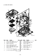
Страница 4: ... 4 ...
Страница 5: ... 5 ...
Страница 6: ... 6 ...
Страница 7: ... 7 ...
Страница 8: ... 8 ...
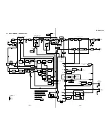
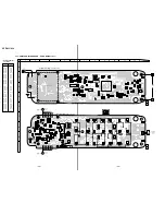
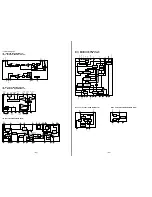
Страница 27: ... 35 SPP 933 934 5 10 SCHEMATIC DIAGRAM BASE KEY Section Page 32 ...