27
SCD-XE600
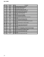
Pin No.
Pin Name
I/O
Description
1
VDD1
–
Power supply terminal (+3.3V)
2
VSS1
–
Ground terminal
3
X1
I
System clock input terminal (5 MHz)
4
X2
O
System clock output terminal (5 MHz)
5
IC
–
Not used
System reset signal input from the reset signal generator “L”: reset
6
RESET
I
For several hundreds msec. after the power supply rises, “L” is input, then it
changes to “H”
7
P27/SCK1
I
Serial data transfer clock signal input from the master controller
8
P26/SI1
I
Serial data input from the master controller
9
P25/SO1
O
Serial data output to the master controller
10
P24/BUSY
I/O
Not used
11
P23
O
LED drive signal output terminal
12
ACK P22
O
Busy signal output to the master controller
13
P21/SO3
I/O
Not used
14
SCK3
I/O
Not used
15
REC P00/INTP0
I
Chip select signal input from the master controller
16
P01/INTP1
I/O
Not used
17
SIRCS P02/TI
I
SIRCS signal input terminal
18
AVSS
–
Ground terminal
19 to 21
ANI3 to ANI1
I
Front panel keys input terminal (A/D input)
22
ANI0
I
Key input terminal (A/D input) Not used
23
VSS0
–
Ground terminal
24
AVDD
–
Power supply terminal (+3.3V)
25
VDD0
–
Power supply terminal (+3.3V)
26
TEST FIP52
I/O
Test mode setting terminal “L”: test mode, normally fixed at “H”
27 to 44
FIP51 to FIP34
I/O
Not used
45 to 58
FIP33 to FIP20
O
Segments drive signal output to the fluorescent indicator tube
59
VDD2
–
Power supply terminal (+3.3V)
60
VLOAD
–
Pull down resistor connection terminal of VFD controller and driver
61 to 64
FIP19 to FIP16
O
Segments drive signal output to the fluorescent indicator tube
65 to 80
FIP15 to FIP0
O
Grid drive signal output to the fluorescent indicator tube
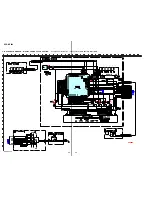
DISPLAY BOARD IC801
µ
PD780232GC-706-8BT (DISPLAY CONTROLLER)


