

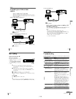
— 4 —
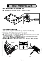
IMPORTANT SERVICE GUIDE
◆
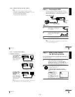
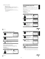
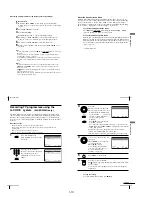
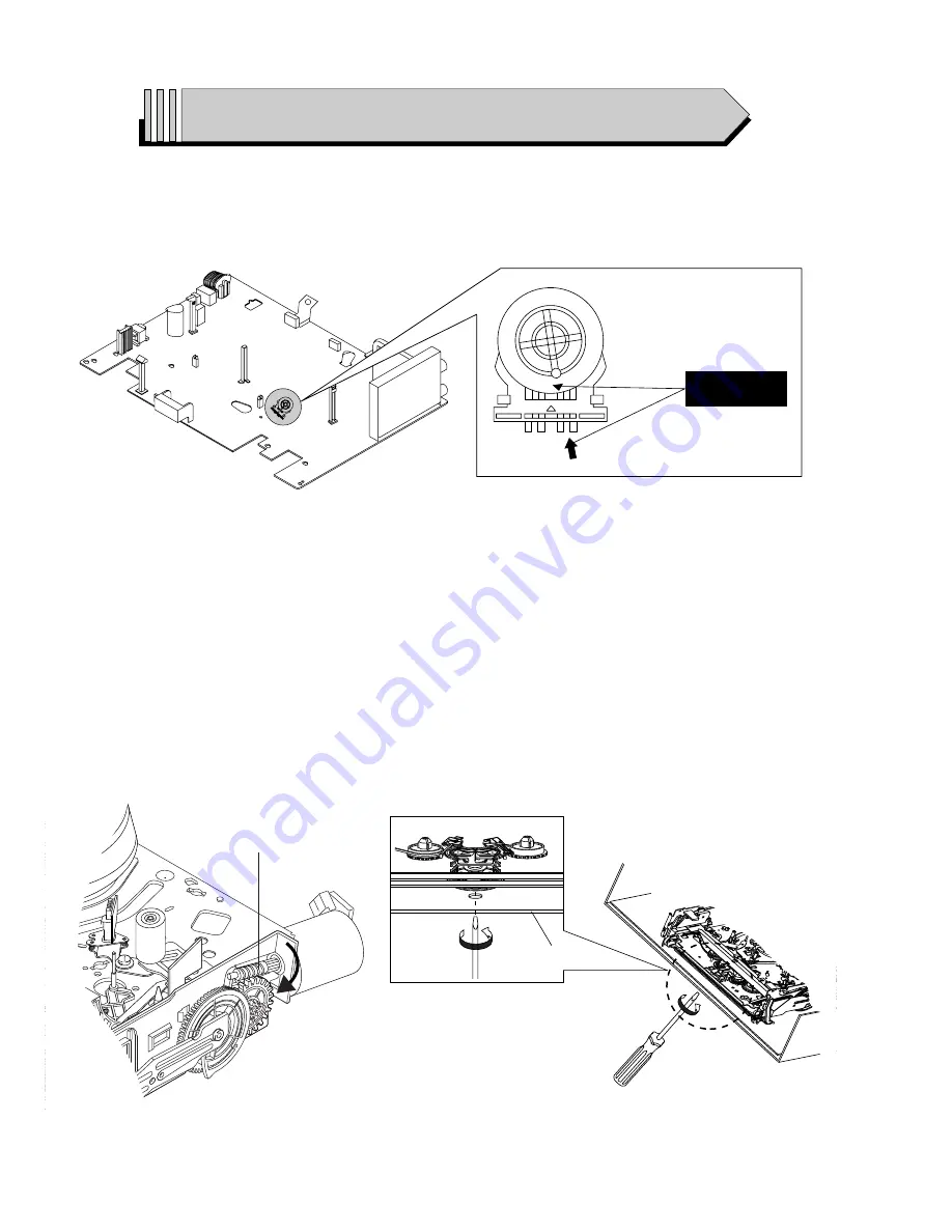
MODE SWITCH (PROGRAM SWITCH) ASSEMBLY POINT
1) When installing the ass’y deck on the Main PCB, be sure to align the assembly point of mode switch.
ASSEMBLY POINT
(ALIGN TWO ARROWS)
Fig. 1
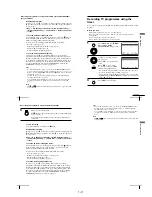
Fig. 2
1
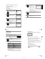
GEAR WORM
Fig. 3
FRAME
◆
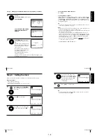
HOW TO EJECT THE CASSETTE TAPE
(If the unit does not operate on condition that tape is inserted into housing ass’y)
1) Turn the Gear Worm
1
clockwise in the direction of arrow with screw driver. (See Fig. 2)
(Other method ; Remove the screw of Motor Load Ass’y, Separate the Motor Load Ass’y)
2) When Slider S, T are approached in the position of unloading, rotate holder Clutch counterclockwise after inserting screw driver in the
hole of frame’s bottom in order to wind the unwiunded tape. (Refer to Fig. 3)
(If you rotate Gear Worm
1
continuously when tape is in state of unwinding, you may cause a tape contamination by grease and
tape damage. Be sure to wind the unwiunded tape in the state of set horizontally.)
3) Rotate Gear Worm
1
clockwise using screw driver again up to the state of eject mode and then pick out the tape. (Refer to Fig. 2)
Содержание RMT-V408A
Страница 28: ...3 1 MAIN PCB AUS 3 3 3 4 COMPONENT SIDE ...
Страница 29: ...3 6 3 5 CONDUCTOR SIDE ...
Страница 30: ...3 2 MAIN PCB E HK ME 3 7 3 8 COMPONENT SIDE ...
Страница 31: ...3 10 3 9 CONDUCTOR SIDE ...
Страница 32: ...3 3 FUNCTION PCB Hi Fi MODEL 3 11 3 12E COMPONENT SIDE CONDUCTOR SIDE ...
Страница 34: ... BLOCK IDENTIFICATION OF MAIN PCB Component Side Conductor Side 4 3 4 4 ...
Страница 35: ...4 1 S M P S AUS PWR OFF PWR ON 1 2 4 6 4 5 ...
Страница 36: ...4 2 S M P S E HK ME 4 7 4 8 PWR OFF PWR ON 1 2 ...
Страница 37: ...4 3 POWER 4 10 4 9 ...
Страница 38: ...6 5 7 3 4 0 8 9 4 4 SYSTEM CONTROL SERVO 4 11 4 12 ...
Страница 41: ... VIDEOPROCESS IN VIDEOPROCESS OUT AUDIOPROCESS IN AUDIOPROCESS OUT qj 4 7 TM BLOCK 4 18 4 17 ...
Страница 42: ... OSD VIDEO PROCESS IN OSD VIDEO PROCESS OUT qk 4 8 OSD VPS PDC 4 19 4 20 ...
Страница 43: ...4 9 A2 NICAM ED925 ED929 EZ725 EZ727 4 21 4 22 ...
Страница 44: ...AUDIO PROCESS OUT AUDIO PROCESS IN VIDEO PROCESS OUT VIDEO PROCESS IN 4 10 INPUT OUTPUT RCA JACK 4 23 4 24 ...
Страница 45: ...4 11 SUB Hi Fi MODEL 4 25 4 26 ...
Страница 48: ...4 32E MEMO ...
Страница 50: ...5 2 PRESS Fig 5 2 Main PCB Top View 5 1 2 Test point location for adjustment mode setting EZ121 EZ424 ...
Страница 51: ...5 3 PRESS Fig 5 3 Main PCB Top View 5 1 3 Test point location for adjustment mode setting ED225 ED323 ...


