


RM-NX7000
9
9
• WAVEFORMS
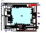
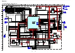
Note on Schematic Diagram:
• All capacitors are in
µ
F unless otherwise noted. pF:
µµ
F 50 WV or
less are not indicated except for electrolytics and tantalums.
• All resistors are in
Ω
and
1
/
4
W or less unless otherwise specified.
•
%
: indicates tolerance.
•
C
: panel designation.
•
A
: B+ Line.
• Power voltage is dc 4.5V and fed with regulated dc power supply
from extermal power voltage jack.
• Voltages and waveforms are dc with respect to ground under no-
signal conditions.
no mark : POWER ON
• Voltages are taken with a VOM (Input impedance 10 M
Ω
).
Voltage variations may be noted due to normal production toler-
ances.
• Waveforms are taken with a oscilloscope.
Voltage variations may be noted due to normal production toler-
ances.
• Circled numbers refer to waveforms.
• IC1 (microcomputer) and IC7 (flash RAM) on Main board cannot
be replaced individually.
Replace it with Main board assembly for service.
*
The voltage and waveform of CSP (chip size package) cannot be
measured, because its lead layout is different form that of
conventional IC.
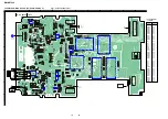
Note on Printed Wiring Board:
•
X
: parts extracted from the component side.
•
Y
: parts extracted from the conductor side.
•
: Pattern from the side which enables seeing.
(The other layers' patterns are not indicated.)
Caution:
Pattern face side:
Parts on the pattern face side seen from the
(Side B)
pattern face are indicated.
Parts face side:
Parts on the parts face side seen from the
(Side A)
parts face are indicated.
• Main boards is six-layer pritnted board.
However, the patterns of layer 2 to 5 have not been included in this
diagrams.
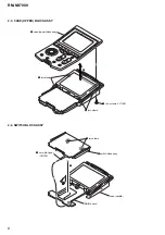
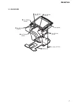
SECTION 4
DIAGRAMS
• IC1 (microcomputer) and IC7 (flash RAM) on Main board
cannot be replaced individually.
Replace it with Main board assembly for service.
– MAIN BOARD –


