
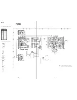

2-1. PRINTED WIRING BOARDS
PS-J10
– 3 –
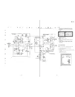
– 4 –
SECTION 2
DIAGRAMS
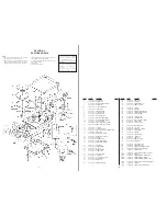
Ref. No.
Location
• Semiconductor
Location
D101
C-3
D102
C-2
D103
C-3
D104
C-2
D105
C-2
IC301
C-7
L1
E-2
L2
E-2
Q301
C-7
ZD1
C-7
• Semiconductor Lead Layouts
Note:
•
X
: parts extracted from the component side.
•
b
: Pattern from the side which enables seeing.
Содержание PS-J10 Primary
Страница 7: ......


