background image

SERVICE MANUAL

Sony Corporation

Audio Business Group
Published by Sony Techno Create Corporation

SPECIFICATIONS

DIGITAL MEDIA PLAYER

9-889-029-01

2008B05-1

© 

2008.02

US Model

NWZ-A726/A726B/A728/A728B/A729

Canadian Model

NWZ-A726/A728

E Model

Australian Model

Tourist Model

East European Model

NWZ-A726/A728/A729

Ver. 1.0  2008.02

NWZ-A726/A726B/A728/

A728B/A729

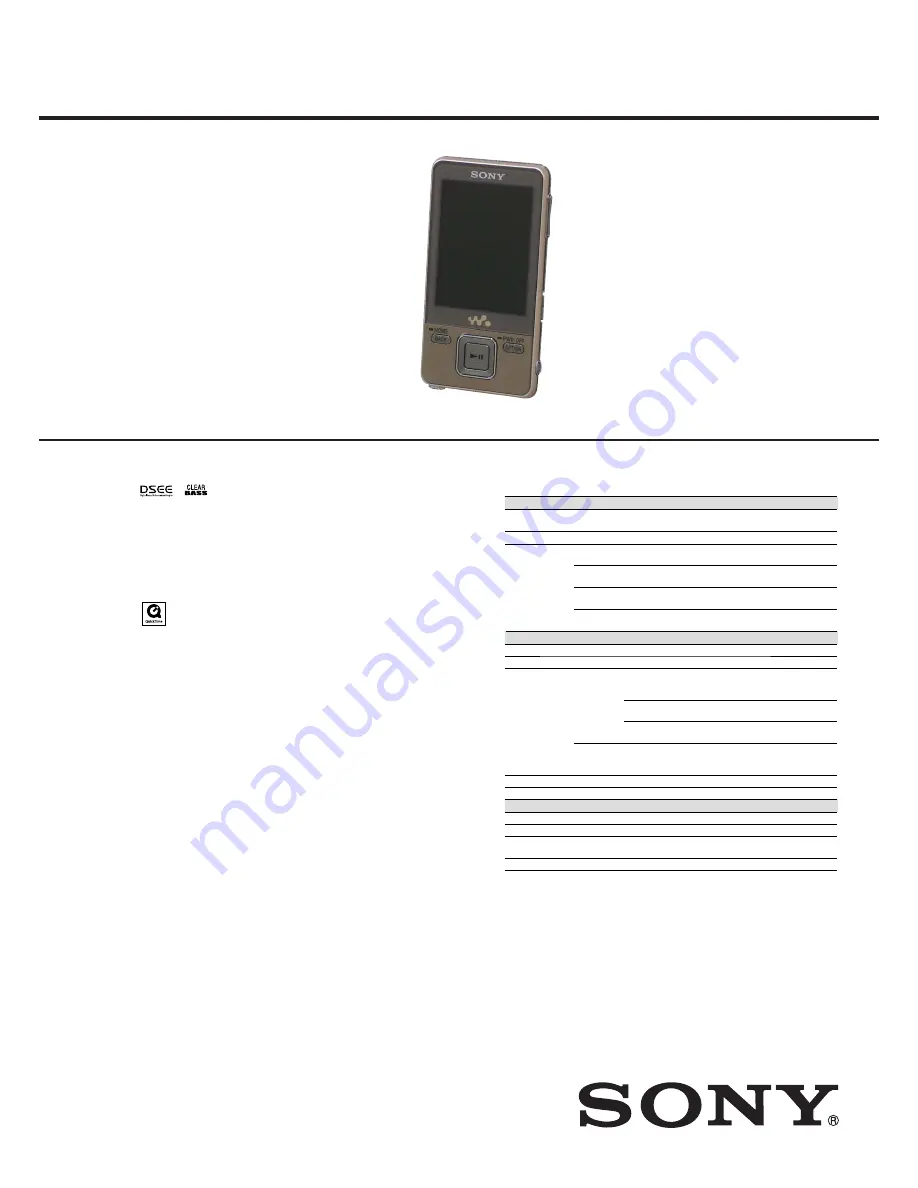
Photo: NWZ-A728

ATRAC is trademark of Sony Corporation.

“WALKMAN” and “WALKMAN” logo are registered trademarks of Sony 
Corporation.

 and 

 are trademarks of Sony Corporation.

Microsoft, Windows, Windows Vista and Windows Media are trademarks or 
registered trademarks of Microsoft Corporation in the United States and/or 
other countries.

Adobe, Adobe Reader and Adobe Flash Player are trademarks or registered 
trademarks of Adobe Systems Incorporated in the United States and/or other 
countries.

MPEG Layer-3 audio coding technology and patents licensed from 
Fraunhofer IIS and Thomson.

IBM and PC/AT are registered trademarks of International Business 
Machines Corporation.

Macintosh is a trademark of Apple Inc.

QuickTime and the QuickTime logo are trademarks or registered trademarks 
of Apple Inc., used under license therefrom.

Pentium is a trademark or a registered trademark of Intel Corporation.

This software is based in part on the work of the Independent JPEG Group.

THIS PRODUCT IS LICENSED UNDER THE MPEG-4 VISUAL PATENT 
PORTFOLIO LICENSE FOR THE PERSONAL AND NON-COMMERCIAL 
USE OF A CONSUMER FOR
(i) ENCODING VIDEO IN COMPLIANCE WITH THE MPEG-4 VISUAL 

STANDARD (“MPEG-4 VIDEO”) AND/OR

(ii) DECODING MPEG-4 VIDEO THAT WAS ENCODED BY A 

CONSUMER ENGAGED IN A PERSONAL AND NON-COMMERCIAL 
ACTIVITY AND/OR WAS OBTAINED FROM A VIDEO PROVIDER 
LICENSED BY MPEG LA TO PROVIDE MPEG-4 VIDEO.

NO LICENSE IS GRANTED OR SHALL BE IMPLIED FOR ANY OTHER 
USE. ADDITIONAL INFORMATION INCLUDING THAT RELATING TO 
PROMOTIONAL, INTERNAL AND COMMERCIAL USES AND 
LICENSING MAY BE OBTAINED FROM MPEG LA, LLC. SEE 
HTTP://WWW.MPEGLA.COM

THIS PRODUCT IS LICENSED UNDER THE AVC PATENT PORTFOLIO 
LICENSE FOR THE PERSONAL AND NON-COMMERCIAL USE OF A 
CONSUMER TO
(i) ENCODE VIDEO IN COMPLIANCE WITH THE AVC STANDARD 

(“AVC VIDEO”) AND/OR

(ii) DECODE AVC VIDEO THAT WAS ENCODED BY A CONSUMER 

ENGAGED IN A PERSONAL AND

NON-COMMERCIAL ACTIVITY AND/OR WAS OBTAINED FROM A 
VIDEO PROVIDER LICENSED TO PROVIDE AVC VIDEO. NO LICENSE 
IS GRANTED OR SHALL BE IMPLIED FOR ANY OTHER USE. 
ADDITIONAL INFORMATION MAY BE OBTAINED FROM MPEG LA, 
L.L.C. SEE HTTP://MPEGLA.COM 

US and foreign patents licensed from Dolby Laboratories. 

All other trademarks and registered trademarks are trademarks or registered 
trademarks of their respective holders. In this manual, 

TM

 and ® marks are not 

specified.

This product is protected by certain intellectual property rights of Microsoft 
Corporation. Use or distribution of such technology outside of this product is 
prohibited without a license from Microsoft or an authorized Microsoft 
subsidiary.

Content providers are using the digital rights management technology for 
Windows Media contained in this device (“WM-DRM”) to protect the integrity 
of their content (“Secure Content”) so that their intellectual property, including 
copyright, in such content is not misappropriated.  
This device uses WM-DRM software to play Secure Content (“WM-DRM 
Software”).  If the security of the WM-DRM Software in this device has been 
compromised, owners of Secure Content (“Secure Content Owners”) may 
request that Microsoft revoke the WM-DRM Software’s right to acquire new 
licenses to copy, display and/or play Secure Content.  Revocation does not alter 
the WM-DRM Software’s ability to play unprotected content.  A list of revoked 
WM-DRM Software is sent to your device whenever you download a license 
for Secure Content from the Internet or from a PC.  Microsoft may, in 
conjunction with such license, also download revocation lists onto your device 
on behalf of Secure Content Owners.

Program ©2008 Sony Corporation
Documentation ©2008 Sony Corporation

Supported file format

Music

File format

MP3(MPEG-1 Layer3) file format, ASF file format, MP4 file format, Wave-Riff file 
format

File extension

MP3 (.mp3), WMA*

1

 (.wma), AAC-LC*

2

 (.mp4, .m4a, .3gp), Linear PCM (.wav)

Codec

MP3

Bit rate: 32 to 320 kbps (Supports variable bit rate (VBR))
Sampling frequency*

3

: 32, 44.1, 48 kHz

WMA*

1

Bit rate: 32 to 192 kbps (Supports variable bit rate (VBR))
Sampling frequency*

3

: 44.1 kHz

AAC-LC*

2

Bit rate: 16 to 320 kbps (Supports variable bit rate (VBR))*

4

Sampling frequency*

3

: 8, 11.025, 12, 16, 22.05, 24, 32, 44.1, 48 kHz

Linear PCM

Bit rate: 1,411 kbps
Sampling frequency*

3

: 44.1 kHz

Video

File format

MP4 file format, “Memory Stick” video format

File extension

.mp4, .m4v

Codec

Video

AVC
(H.264/AVC)

Profile: Baseline Profile
Level: Max. 1.3
Bit rate: Max. 768 kbps

MPEG-4

Profile: Simple Profile
Bit rate: Max. 2,500 kbps

Frame rate: Max. 30 fps
Resolution: Max. QVGA (320 × 240)

Audio

AAC-LC

Channel number: Max. 2 channels
Sampling frequency*

3

: 24, 32, 44.1, 48 kHz

Bit rate: Max. 288 kbps per 1 channel

File size

Max. 2 GB

The number of files

Max. 1,000

Photo

*

5

File format

Compatible with DCF 2.0/Exif 2.21file format

File extension

.jpg

Codec

Profile: Baseline Profile
Number of pixels: Max. 4,000 × 4,000 pixels (16,000,000 pixels)

The number of files

Max. 10,000

*

1

WM-DRM 10 files are compatible.

*

2

Copyright protected AAC-LC files cannot be played back.

*

3

Sampling frequency may not correspond to all encoders.

*

4

Non-standard bit rates or non-guaranteed bit rates are included depending on the 
sampling frequency.

*

5

Some photo files cannot be played back, depending on their file formats.

– Continued on next page –

Содержание NWZ-A726B Marketing Specifications (Black)

Страница 1: ...rks are not specified This product is protected by certain intellectual property rights of Microsoft Corporation Use or distribution of such technology outside of this product is prohibited without a license from Microsoft or an authorized Microsoft subsidiary Content providers are using the digital rights management technology for Windows Media contained in this device WM DRM to protect the integ...

Страница 2: ... 8 GB Approx 7 30 GB 7 840 890 880 bytes 1 Available storage capacity of the player may vary A portion of the memory is used for data management functions Output headphones Frequency response 20 to 20 000 Hz when playing data file single signal measurement Interface Headphone Stereo mini jack WM PORT multiple connecting terminal 22 pins Hi Speed USB USB 2 0 compliant Operating temperature 5 C to 3...

Страница 3: ...s etc Usable with ordinary solder It is best to use only unleaded solder but unleaded solder may also be added to ordinary solder NOTE THE CN601 CN602 IC301 IC302 IC305 IC501 IC503 IC508 IC509 IC601 IC602 IC701 IC751 IC752 IC901 AND IC902 ON THE MAIN BOARD REPLAC ING CN601 CN602 IC301 IC302 IC305 IC501 IC503 IC508 IC509 IC601 IC602 IC701 IC751 IC752 IC901 and IC902 on the MAIN board cannot exchang...

Страница 4: ...he Home menu appears Press the button to select Settings and then press the button to confirm Press the button to select Common Settings and then press the button to confirm The list of Common Settings options appears Press the button to select Format and then press the button to confirm All data including songs will be deleted Proceed appears Press the button to select Yes and then press the butt...

Страница 5: ...r enters standby mode If you press any button while the player is in standby mode the Now Playing screen etc appears and the player is ready for operation Furthermore if you leave the player in standby mode for about a day the player turns completely off automatically If you press any button when the player is turned off the start up screen appears first then the Now Playing screen appears Note Th...

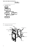
Страница 6: ... DISASSEMBLY FLOW Note Follow the disassembly procedure in the numerical order given 3 2 COVER REAR REAR ASSY SET 3 2 COVER REAR REAR ASSY Page 6 3 3 BATTERY Page 7 3 4 MAIN BOARD Page 7 3 5 LCD ASSY Page 8 two screws M1 4 two ornamental screws screw M1 4 two claws rear assy two claws lid ACC claw claw cover rear ...

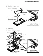
Страница 7: ...ng battery connector please be careful about the color of the lead wires as shown in a figure and install battery connector screw B1 4 spacer line in claw BATT wire sheet R connector CN601 connector board to board connector board to board spacer line in connector CN901 HP flexible print board CN301 RI MAIN board RB cushion PWB sheet key CN602 escutcheon CN RT spacer PWB S RE sheet WM P RG cushion ...

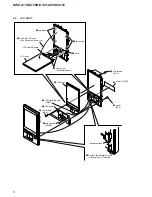
Страница 8: ... two claws SW board LCD flexible board CN801 sheet LCD B two screws B1 4 screw B1 4 RE LCD assy R Open the LCD assy in the direction of the arrow waterproof jack Remove the waterproof jack in the direction of the arrow RB boss RT Pull out the LCD flexible board LCD flexible board LCD assy ...

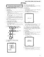
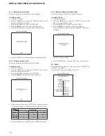
Страница 9: ...E BATTCHK DAC SHUTDOWN EXITTEST 4 1 1 Power supply voltage check This mode is used in case power supply voltage in the state where all power supply lines are starting is checked Checking method 1 Enter the test mode 2 Press the v V key to select the POWER and press the B key to enter the minor item 3 Press the v V key to select the VCHK 4 Press the u key all power supply lines are started liquid c...

Страница 10: ...s state each time the OPTION key is pressed the port setting for the charge is changed as shown in the table below Port control Display CHG_XCHGEN CHG_PEN1 CHG_PEN2 AC L H H USB500 L H H USB100 L H L 6 Press the BACK key return to minor item selection screen 4 1 5 Battery voltage detection check This mode is used in case battery voltage is checked Checking method 1 Enter the test mode 2 Press the ...

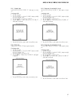
Страница 11: ...finity Zero HPOUT VOL 30 START 5 Press the BACK key return to minor item selection screen 4 2 3 Frequency characteristic 1 check 20 Hz 0 dBs L ch R ch VOLUME 25 audio signal is output ted Checking method 1 Enter the test mode 2 Press the v V key to select the AUDIO and press the B key to enter the minor item 3 Press the v V key to select the F1 4 Press the u key 20 Hz 0 dBs L ch R ch VOLUME 25 aud...

Страница 12: ... Maximum output check 1 kHz 0 dBs L ch R ch VOLUME 30 Headphone output when AVLS operates 1 kHz 0 dBs L ch R ch VOLUME 13 audio signal is outputted Checking method 1 Enter the test mode 2 Press the v V key to select the AUDIO and press the B key to enter the minor item 3 Press the v V key to select the MAXOUT 4 Press the u key 1 kHz 0 dBs L ch R ch VOLUME 30 Headphone output when AVLS operates 1 k...

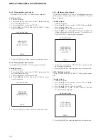
Страница 13: ...the following order All black default All red All green All blue All white Color bar Maximum drawing size confirmation diagonal gradation red diagonal gradation green diagonal gradation blue diagonal gradation white Maximum drawing size confirmation All blue All sides are red is displayed Whether red in all sides is seen is confirmed 5 In this state each time the VOL key is pressed LCD back light ...

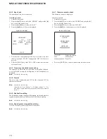
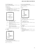
Страница 14: ...ormat The user s area is formatted and ICV for the video and ICV for audio are initialized Note Not used for the servicing Format the set from Settings Common settings For mat when it home menu in usually operates when the set should format it 4 4 5 Destination setting The destination setting language information and sound pressure regulation information are written in the NAND flash memory Note N...

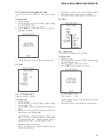
Страница 15: ...lection screen 4 5 CLESTE liquid crystal display MPTAPP MENU POWER AUDIO VIDEO OTHER CLESTE WCABLE DAC WOCABLE SHUTDOWN EXITTEST 4 5 1 Clear stereo setting With cable This mode is according to an original sound playback for adjust ment to right and left sound Note Not used for the servicing 4 5 2 Clear stereo setting No cable This mode is according to an original sound playback for adjust ment to ...

Страница 16: ...16 NWZ A726 A726B A728 A728B A729 MEMO ...

Страница 17: ...7 SDR_BA1 T4 BA1 H8 SDR_CLK AA5 CLK J1 SDR_CSZ0 T3 CS J8 SDR_CKE0 T1 CKE J2 SDR_WEZ R5 WE K8 SDR_CASZ U8 CAS K7 SDR_RASZ T5 RAS J9 SDR_DQM0 P5 DQM0 K9 SDR_DQM1 R4 DQM1 K1 SDR_DQM2 R3 DQM2 F8 SDR_DQM3 R2 DQM3 F2 A0 A12 SDR_D0O SDR_D31 SDR_A00 SDR_A12 NAND FLASH MEMORY IC751 NAND_DA0 NAND_DA7 NAND_ALE D3 I O1 I O8 ALE 17 NAND_CLE E9 CLE 16 NAND_CEZ0 M9 XCE1 9 NAND_CEZ1 C2 XCE2 10 NAND_CEZ2 B3 NAND_C...

Страница 18: ... LX1 20 EN 31 Y2 CISET 12 DOK CHG_XCHGEN 10 V10 CEN CHG_PEN2 40 W8 PEN2 USB_SUSPEND 1 AB8 USUS XCHG_DET 39 AC4 CST1 CHG_XFLT 37 AB4 U70_SOUT T17 U70_SRIN T18 CRD_DET AB3 CRD_AD C8 CST2 VOLTAGE DETECT IC902 CHARGE CONTROL Q901 TXD_PUCTL AB2 3 1V REGULATOR IC602 1 8V REGULATOR IC504 3 1V REGULATOR IC503 HP WM PORT 1 8V 1 8V REGULATOR IC301 VDD_ANA_F VDD_ECO_J VDD_GP1_J VDD_GP1_FB_J VDD_GP3 VDD_GP5 V...

Страница 19: ...erances Circled number refer to waveform Signal path F AUDIO L VIDEO The voltage and waveform of CSP chip size package cannot be measured because its lead layout is different form that of conventional IC THIS NOTE IS COMMON FOR PRINTED WIRING BOARDS AND SCHEMATIC DIAGRAMS In addition to this the necessary note is printed in each block For Printed Wiring Boards Note Y parts extracted from the condu...

Страница 20: ...W16 W14 W15 W13 W11 W12 2 4 3 1 2 4 3 1 6 10 1 5 H8 G8 F8 E8 D8 C8 B8 A8 H7 G7 F7 E7 D7 C7 B7 A7 H6 G6 F6 E6 D6 C6 B6 A6 H5 G5 F5 C5 B5 A5 H4 G4 F4 C4 B4 A4 H3 G3 F3 E3 D3 C3 B3 A3 H2 G2 F2 E2 D2 C2 B2 A2 H1 G1 F1 E1 D1 C1 B1 A1 5 1 3 4 A1 B1 C1 D1 E1 F1 G1 H1 J1 K1 L1 M1 N1 P1 R1 A2 B2 C2 D2 E2 F2 G2 H2 J2 K2 L2 M2 N2 P2 R2 A3 B3 C3 D3 E3 F3 G3 H3 J3 K3 L3 M3 N3 P3 R3 A7 B7 C7 D7 E7 F7 G7 H7 J7 K...

Страница 21: ... R775 R776 R777 R778 R779 R780 R781 C752 C753 C754 C755 IC301 IC302 IC503 IC504 IC508 IC509 R205 FB601 24 25 1 48 24 25 1 48 1 B2 B1 A2 A1 3 1 4 6 7 B2 B1 A2 A1 1 3 4 6 1 2 1 2 4 A1 A2 B1 C1 C2 B2 3 2 1 11 1 2 10 A A 41 30 1 40 31 21 10 11 20 MAIN BOARD SIDE B 1 875 443 11 11 A B C D E F G H I 1 2 3 4 5 6 7 8 9 10 11 12 13 14 15 16 RESET SHEET KEY LITHIUM ION STORAGE BATTERY 3 7V 610mAh CHASSIS CH...

Страница 22: ...R_D25 SDR_D24 SDR_D23 SDR_D22 SDR_D21 SDR_D20 SDR_D02 SDR_D19 SDR_D18 SDR_D17 SDR_D16 SDR_D15 SDR_D14 SDR_D13 SDR_D12 SDR_D11 SDR_D10 SDR_D01 SDR_CLK VDD_L0_F VDD_GP1_J SDR_D00 SDR_XCS0 CHG_PEN2 CHG_XCHGEN USB_SUSPEND KEY_WAKE VDD_GP3 XHOLD_KEY KEY_AD1 CPU_REFCLKO HP_XMUTE ADA_XRST XCRD_LINEOUT PCM0_DADT WAKEUP_INT CHG_ICTL CRD_AD AB0_A1 AB0_A3 AB0_A4 AB0_A5 AB0_A6 AB0_A7 AB0_A8 AB0_XCS2 AB0_D0 AB...

Страница 23: ...A04 SDR_CLK SDR_D31 SDR_A08 SDR_D26 SDR_A01 C701 0 1 DGND C703 0 1 C705 0 1 C707 0 1 C709 0 1 C711 0 1 C713 0 1 VDD_ECO_J FL701 100k R702 SDR_D17 SDR_A06 SDR_D02 SDR_XWR SDR_A12 SDR_D20 SDR_A05 SDR_D13 SDR_DQM3 SDR_DQM2 SDR_A04 SDR_D10 SDR_DQM2 SDR_BA0 SDR_D16 SDR_D21 SDR_DQM1 SDR_DQM0 SDR_A10 SDR_D22 SDR_XWR SDR_A09 SDR_D23 SDR_XRAS SDR_A08 SDR_D24 SDR_XCAS SDR_A07 SDR_D25 SDR_BA1 SDR_A06 SDR_D26...

Страница 24: ... NAND_ALE NAND_XWR NAND_XWP NAND_RXB1 NAND_XCS1 NAND_RXB1 NAND_XCS1 NAND_RXB1 NAND_RXB2 NAND_XRD NAND_XCS2 NAND_XCS1 NAND_D07 NAND_D06 NAND_D05 NAND_D04 NAND_D03 NAND_D02 NAND_D01 NAND_D00 NAND_RXB3 NAND_XCS0 NAND_XWR NAND_XCS3 NAND_RXB3 NAND_D00 NAND_D01 NAND_D02 NAND_D03 NAND_D04 NAND_D05 NAND_D06 NAND_D07 NC NC NC NC NC NC NC NC NC NC NC NC NC NC NC NC NC NC NC NC NC NC PSL NC NC NC NC NC R B2 ...

Страница 25: ...19 220k IC502 TC7SG08AFS 1 2 GND 3 4 5 VCC IC504 TK63718HCL G 1 VIN 2 GND 3 VOUT 4 NC 5 GND 6 VCONT R521 0 R522 0 0 1 C505 0 1 C507 0 1 C508 0 1 C509 FL501 CL501 CL502 VDD_GP1_FB_J SN74AVC1T45YZPR IC509 A1 VCCA B1 GND C1 A C2 B B2 DIR A2 VCCB 0 1 C517 0 1 C518 R527 0 AB0_XDMARQ AB0_XDACK R510 22 R528 0 VDD_GP1_J TC7SG04AFS IC508 1 2 GND 3 NC 4 5 VCC 0 1 C516 100k R520 AB0_XRD AB0_A2 AB0_A3 AB0_A4 ...

Страница 26: ...M2 7 NC2 8 VCC 9 NC1 10 COM1 C208 0 1 R106 5 6 R206 5 6 11P CN301 1 MIC_RIN 2 MIC_RIN 3 HP_R 4 HP_R 5 COM 6 COM 7 COM 8 MIC_L 9 MIC_L 10 HP_L 11 HP_L R123 0 R223 0 150k R304 220k R305 220 R315 47 R105 47 R205 0 001 C301 470 R220 470 R120 0 0047 C116 0 0047 C216 1k R313 1k R307 D301 VMZ6 8NT2L CL102 CL202 0 47 C326 6 3V C316 22 0 C327 0 C328 0 C329 0 C330 EN1 GND VOUT2 VOUT1 VSS EN2 VIN MUTING MUTI...

Страница 27: ... LX1 24 PG1 31 CISET 32 CT 41 EP 33 THM 34 BAT 35 SYS 36 PEN1 37 CST2 38 UOK 39 CST1 40 PEN2 9 PV2 10 CEN 17 BVSET 18 GND 19 FB1 20 EN 25 PG3 26 LX3 27 PV3 28 VL 29 FB3 30 DISET 0 R931 0 R930 0 R928 R912 0 0 R901 0 R906 0 R907 R904 0 0 R929 FB852 0 VDR851 470p C855 LINE_OUT_R USB_DP R855 47k DBG_UART_TXD CRD_DET USB_DM D851 RB060M 30TR FB857 0 R853 1k R851 1k CRD_AD LF851 DBG_UART_RXD R857 470k 0 ...

Страница 28: ...N881 1 KEY_AD0 3 KEY_AD1I 5 SPI0_LCD_XCS 7 DGND 9 LCD_BLTCTL 11 LCD_PWM1 13 DGND 15 VDD_UNREG_J 17 LCD_B0 19 LCD_B1 21 LCD_B2 23 LCD_B3 25 LCD_B4 27 LCD_B5 29 LCD_ENABLE 31 LCD_PXCLK 33 LCD_HSYNC 35 LCD_VSYNC 37 LCD_PON 39 VDD_ANA_F 41 VDD_LOG_F 2 KEY_GND 4 KEY_AD1O 6 KEY_WAKE 8 DGND 10 SPI0_MOSI 12 SPI0_CLK 14 DGND 16 VDD_UNREG_J 18 LCD_G5 20 LCD_G4 22 LCD_G3 24 LCD_G2 26 LCD_G1 28 LCD_G0 30 LCD_...

Страница 29: ...G4 LCD_VSYNC JL803 FB819 SSM3K15FV TL3SONYZ Q801 S LCD_G1 LCD_B3 FB813 JL804 LCD_PXCLK FB807 SPI0_MOSI 3300 R804 VDD_UNREG_J 100k R830 VDD_ANA_F FL801 JL801 LCD_ENABLE 1 C803 FB814 SPI0_LCD_XCS 100k R829 0 R810 FB808 FB802 TPS60231RGTR IC801 1 ISET 2 NC 3 NC 4 D3 5 D2 6 D1 7 PGND 8 VOUT 10 C1 11 C1 12 C2 13 VIN 14 GND 15 EN1 16 EN2 9 C2 LCD_R1 FB815 0 R808 0 R809 0 R803 R1 B3 B2 SDI G4 R4 B4 DEN G...

Страница 30: ...5 S896 CL888 17 1 4 5 8 S G D 12 9 16 13 R801 R803 FB814 R804 FB815 FB816 FB817 FB818 R808 FB819 R809 R810 CN801 R829 R830 R831 1 2 39 38 C801 C803 C804 C805 C806 CN881 41 42 1 2 IC801 Q801 FL801 SW BOARD SIDE A SW BOARD SIDE B 1 875 442 11 11 1 875 442 11 11 A B C D 1 2 3 4 5 6 7 8 9 10 11 12 13 LCD ASSY HOME BACK PWR OFF OPTION A MAIN BOARD CN601 Note CN801 CN881 and IC801 on the SW board cannot...

Страница 31: ...D11 CD10 CD9 XI XO G3 XRD TEST MUX H1 TESTEN H8 ATPGEN A8 BURNIN MACRO DEVICE SERIAL INTERFACE ENGINE HOST SERIAL INTERFACE ENGINE A6 R1 A3 DP A4 DM B1 VBUSFLG C1 VBUSEN C3 VBUS D1 XRESET D8 CLKIN CONTROLLER FIRST IN FIRST OUT USB DMA CONTROLLER H3 XWRL VSS G7 B7 B6 B5 B4 B2 CVDD D7 LVDD G2 LVDD C7 LVDD A7 LVDD A2 HVDD C2 HVDD B3 HVDD A5 H7 CD8 F6 G6 H6 E6 F5 H5 G5 CD7 CD6 CD5 CD4 CD3 CD2 CD1 C4 C...

Страница 32: ... PG1 23 LX1 22 PV1 21 SSKP 4 FB5 5 PV5 6 OUT5 7 PG2 8 LX2 9 PV2 20 EN 16 PV4 15 OUT4 14 BP 11 FB2 3 USB 34 BAT 10 CEN 3 3V LOW DROPOUT HIGHEST VOLTAGE SELECTOR REG1 DC DC CONVERTER REG3 DC DC CONVERTER REG4 LOW DROPOUT REG5 LOW DROPOUT REG2 DC DC CONVERTER 14 GND 15 EN1 16 EN2 13 VIN 11 C1 12 C2 10 C1 9 C2 2 NC 1 ISET 3 NC 4 D3 6 D1 5 D2 8 VOUT 7 PGND CHARGE PUMP CURRENT SINKS CONTROL REFERENCE SW...

Страница 33: ...nector 12 VA Power supply terminal 1 8V 13 AGND Ground terminal 14 DAC_FILT O Positive reference voltage output terminal 15 VQ O Quiescent voltage output terminal 16 ADC_FILT O Positive reference voltage output terminal 17 MICIN1 AIN3A I Microphone signal input terminal Not used 18 MICIN2 AIN3B BIAS I Microphone signal input terminal Not used 19 AIN2A I Analog audio L ch signal input terminal Not ...

Страница 34: ...13 SWGND Ground terminal B14 NC Not used B15 SWADP2 Not used B16 GND Ground terminal B17 VCCADP I Power supply input terminal 5V B18 NC Not used B19 IO_A Not used B20 VDD_L0 I Power supply input terminal 1 2V B21 to B26 NC Not used C1 NC Not used C2 NAND_CEZ1 O Chip enable signal output to the NAND flash memory NWZ A728 A728B A729 only C3 NAND_CEZ3 O Chip enable signal output to the NAND flash mem...

Страница 35: ...IO_B Not used E6 NAND_DA5 I O Two way data bus with the NAND flash memory E7 NC Not used E8 NAND_DA7 I O Two way data bus with the NAND flash memory E9 NAND_CLE O Command latch enable signal output to the NAND flash memory E10 BATSEL Not used E11 SWBAT Not used E12 CAPBTDL Not used E13 CAPADDL Not used E14 NC Not used E15 SWVBUS Not used E16 E17 NC Not used E18 AB0_A4 O Address signal output to th...

Страница 36: ...be signal output to the USB controller J22 to J24 AB0_D10 to AB0_D12 I O Two way data bus with the USB controller J25 CHGGND1 Ground terminal J26 NC Not used K1 to K3 VDD_L1 I Power supply input terminal 1 2V K4 K5 SDR_DATA28 SDR_DATA26 I O Two way data bus with the SD RAM K8 NAND_RBZ3 O Read busy signal output to the NAND flash memory NWZ A728 A728B A729 only K9 NAND_DA6 I O Two way data bus with...

Страница 37: ...isplay P23 LCD_PXCLK O Pixel clock signal output to the liquid crystal display P24 NC Not used P25 P26 IO_A Not used R1 SDR_DATA0 I O Two way data bus with the SD RAM R2 to R4 SDR_DQM3 to SDR_DQM1 O Write mask signal output to the SD RAM R5 SDR_WEZ O Write enable signal output to the SD RAM R8 SDR_DATA1 I O Two way data bus with the SD RAM R9 GND Ground terminal R10 NC Not used R17 U70_CTSZ Not us...

Страница 38: ...ack light control signal output to the LED control V18 UART_SEL Not used V19 NCHP_DET I Headphone detection signal input terminal Not used V22 C_RTCK I Clock signal input terminal for JTAG V23 C_TRSTZ I Reset signal input terminal for JTAG V24 VPLLIN I Power supply input terminal 2V V25 VDSPIN I Power supply input terminal 2 9 4 2V V26 VDSP Not used W1 IOGND Ground terminal W2 NC Not used W3 LCD_P...

Страница 39: ... R sampling clock signal input from the A D D A converter AB23 AB24 GND Ground terminal AB25 GND1 Ground terminal AB26 OSCIN I Sub system clock input terminal 32 768 kHz AC1 to AC3 IO_A Not used AC4 XCHG_DET I Charge detection signal input from the power control AC5 USB_INT1 I Interrupt request signal input from the USB controller AC6 SPIO_XCS0 O Chip select signal output to the liquid crystal dis...

Страница 40: ...V AE5 DD2GNDA Ground terminal AE6 DD2INA I Power supply input terminal 2 9 4 2V AE7 VDD_L0 I Power supply input terminal 1 2V AE8 VDD_L1 I Power supply input terminal 1 2V AE9 IO_C Not used AE10 AE11 NC Not used AE12 DD1INA I Power supply input terminal 2 9 4 2V AE13 IO_B Not used AE14 AVDD_LPLL I Power supply input terminal 1 2V AE15 AVDD_HPLL I Power supply input terminal 1 2V AE16 GND Ground te...

Страница 41: ... DD1INB2 I Power supply input terminal 2 9 4 2V AF18 DD1VFBK2 I Power supply voltage feedback terminal AF19 DD1GNDA Ground terminal AF20 VGP1 O Power supply output terminal 2 85V AF21 COM Not used AF22 NC Not used AF23 VGP3 O Power supply output terminal 2 85V AF24 to AF26 NC Not used ...

Страница 42: ... difference from the original one Items marked are not stocked since they are seldom required for routine ser vice Some delay should be anticipated when ordering these items The mechanical parts with no reference number in the exploded views are not sup plied Color Indication of Appearance Parts Ex ample KNOB BALANCE WHITE RED R R Parts Color Cabinet s Color Accessories are given in the last of th...

Страница 43: ...US CircuitCity 51 X 2190 943 1 REAR ASSY BLACK NWZ A728 CND 51 X 2190 944 1 REAR ASSY PINK NWZ A728 CND 51 X 2190 945 1 REAR ASSY BLACK NWZ A728 E AUS JE 51 X 2190 946 1 REAR ASSY WHITE NWZ A728 E AUS JE 51 X 2190 947 1 REAR ASSY PINK NWZ A728 E AUS JE 51 X 2190 948 1 REAR ASSY BLACK NWZ A728 MX3 51 X 2190 949 1 REAR ASSY BLACK NWZ A728 EE 51 X 2190 950 1 REAR ASSY SILVER NWZ A728 EE 51 X 2190 951...

Страница 44: ...E MX3 AUS JE 103 X 2190 629 1 MAIN BOARD COMPLETE for SERVICE 8G NWZ A728 E MX3 AUS JE 103 X 2190 630 1 MAIN BOARD COMPLETE for SERVICE 16G NWZ A729 E AUS JE 103 X 2190 631 1 MAIN BOARD COMPLETE for SERVICE 4G NWZ A726B 103 X 2190 632 1 MAIN BOARD COMPLETE for SERVICE 8G NWZ A728B 104 3 254 136 01 SCREW B1 4 105 3 279 352 01 SHEET BATT ADHESIVE 106 1 756 702 11 BATTERY LITHIUM ION STRAGE E MX3 AUS...

Страница 45: ... 334 01 BUTTON VOL VOL 157 3 398 061 01 SHEET OB ADHESIVE 158 3 234 449 27 SCREW M1 4 159 A 1506 857 A SW BOARD COMPLETE 160 X 2190 604 1 LCD ASSY 161 3 279 351 01 CONNECTOR A RUBBER 162 1 875 533 11 HP FLEXIBLE PRINT BOARD 163 3 279 342 01 PLATE HP FIXED 164 3 254 135 01 SCREW B1 4 165 3 398 056 01 SHEET LCD B 166 3 254 136 01 SCREW B1 4 167 3 874 255 01 SHEET WR 168 3 279 340 01 CHASSIS MAIN 169...

Страница 46: ...1 112 716 11 CERAMIC CHIP 0 1uF 10 6 3V C509 1 112 716 11 CERAMIC CHIP 0 1uF 10 6 3V C510 1 112 716 11 CERAMIC CHIP 0 1uF 10 6 3V C511 1 112 717 91 CERAMIC CHIP 1uF 10 6 3V C512 1 112 717 91 CERAMIC CHIP 1uF 10 6 3V C516 1 112 716 11 CERAMIC CHIP 0 1uF 10 6 3V C517 1 112 716 11 CERAMIC CHIP 0 1uF 10 6 3V C518 1 112 716 11 CERAMIC CHIP 0 1uF 10 6 3V C601 1 112 717 91 CERAMIC CHIP 1uF 10 6 3V C602 1...

Страница 47: ... 506 91 CERAMIC CHIP 1uF 20 6 3V C917 1 125 777 11 CERAMIC CHIP 0 1uF 10 10V C918 1 125 777 11 CERAMIC CHIP 0 1uF 10 10V C919 1 112 746 11 CERAMIC CHIP 4 7uF 10 6 3V C920 1 112 815 91 CERAMIC CHIP 10uF 20 6 3V C921 1 112 815 91 CERAMIC CHIP 10uF 20 6 3V C922 1 125 777 11 CERAMIC CHIP 0 1uF 10 10V C924 1 164 937 11 CERAMIC CHIP 0 001uF 10 50V C925 1 112 815 91 CERAMIC CHIP 10uF 20 6 3V CONNECTOR CN...

Страница 48: ...4 1 218 990 81 SHORT CHIP 0 R605 1 218 990 81 SHORT CHIP 0 R606 1 208 911 11 METAL CHIP 10K 0 5 1 16W R607 1 218 985 11 RES CHIP 470K 5 1 16W R608 1 218 953 11 RES CHIP 1K 5 1 16W R611 1 218 990 81 SHORT CHIP 0 R615 1 218 953 11 RES CHIP 1K 5 1 16W R616 1 245 684 21 RES CHIP 0 22 5 1 8W R617 1 245 684 21 RES CHIP 0 22 5 1 8W R618 1 218 990 81 SHORT CHIP 0 R619 1 218 990 81 SHORT CHIP 0 R620 1 218 ...

Страница 49: ...0 5 1 16W R923 1 208 695 11 METAL CHIP 3 3K 0 5 1 16W R926 1 208 911 11 METAL CHIP 10K 0 5 1 16W R927 1 208 931 11 METAL CHIP 68K 0 5 1 16W R928 1 218 990 81 SHORT CHIP 0 R929 1 216 864 11 SHORT CHIP 0 R930 1 218 990 81 SHORT CHIP 0 R931 1 218 990 81 SHORT CHIP 0 R935 1 218 990 81 SHORT CHIP 0 SWITCH S601 1 572 938 21 SWITCH TACTIL RESET S602 1 771 449 11 SWITCH SLIDE HOLD TERMINAL TB301 1 780 112...

Страница 50: ...2 31 MANUAL QSG INSTRUCTION Quick Start Guide SPANISH NWZ A726 MX3 NWZ A728 MX3 3 299 382 41 MANUAL QSG INSTRUCTION Quick Start Guide PORTUGUESE NWZ A726 MX3 NWZ A728 MX3 3 299 382 51 MANUAL QSG INSTRUCTION Quick Start Guide SIMPLIFIED CHAINESE NWZ A726 E AUS JE NWZ A728 E AUS JE NWZ A729 E AUS JE 3 299 382 61 MANUAL QSG INSTRUCTION Quick Start Guide TRADITIONAL CHAINESE NWZ A726 E AUS JE NWZ A728...

Страница 51: ...MEMO NWZ A726 A726B A728 A728B A729 51 ...

Страница 52: ...29 REVISION HISTORY Checking the version allows you to jump to the revised page Also clicking the version at the top of the revised page allows you to jump to the next revised page Ver Date Description of Revision 1 0 2008 02 New ...

Отзывы: