background image

27

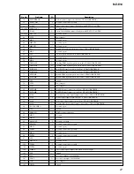
MZ-E10

50

XSLP MTR OP

O

Start/stop signal output to motor drive (CXA8125ER-TBM-E)

51

XDISC DET

I

Not used (connected to ground)

52

D_EN2

O

Drive control signal output to Headphone AMP (NJU-8713V-TE2)

53 to 56

SMON 0 to 3

Not used (open)

57

F16M

O

Clock (16.9344MHz) output to Headphone AMP (NJU-8713V-TE2)

58 to 61

MD 7 to 4

Not used (open)

62

VCC2

Power supply

63

MD3

Not used (open)

64

MECNT0

I

Not used (open)

65

MECNT1

Not used (open)

66

FG

I

Spindle FG signal input from motor drive (CXA8125ER-TBM-E)

67

MD2

Not used (open)

68

4M

O

Clock output to motor drive (CXA8125ER-TBM-E)

69

MD1

Not used (open)

70

MD0

Not used (open)

71

TRPWMF

O

Tracking PWM signal output to motor drive (CXA8125ER-TBM-E)

72

TRPWMR

O

Tracking PWM signal output to motor drive (CXA8125ER-TBM-E)

73

FOPWMF

O

Focus PWM signal output to motor drive (CXA8125ER-TBM-E)

74

FOPWMR

O

Focus PWM signal output to motor drive (CXA8125ER-TBM-E)

75

SPPWMF

O

Spindle PWM signal output to motor drive (CXA8125ER-TBM-E)

76

SPPWMR

O

Spindle PWM signal output to motor drive (CXA8125ER-TBM-E)

77

VSS

Ground

78

VCC2

Power supply

79

VDD

Power supply

80

SLPWMF

O

Sled PWM signal output to motor drive (CXA8125ER-TBM-E)

81

SLPWMR

O

Sled PWM signal output to motor drive (CXA8125ER-TBM-E)

82

SLD0

O

Sled stepping control signal output to motor drive (CXA8125ER-TBM-E)

83

SLD1

I

Sled FG signal input from motor drive (CXA8125ER-TBM-E)

84

SLD2

O

Sled control signal output to motor drive (CXA8125ER-TBM-E)

85

SLD3

O

Stepping /DC change signal output to motor drive (CXA8125ER-TBM-E)

86

(LOCAL CHK3)

Not used (open)

87

VSS

Ground

88

HOLD SW

I

HOLD switch signal input

89

MD15

Not used

90

MD14

Not used

91

XADJUST

I

Test mode set input

92

XPATCH

I

Not used (connected to ground)

93

MD13

Not used (open)

94

TYPE3

I

Not used (connected to ground)

95

MD12

Not used (open)

96

TYPE2

I

Not used (connected to ground)

97

VSS

Ground

98 to 101

MD11 to 8

Not used (open)

102

TYPE1

I

Not used (connected to ground)

103

TYPE0

I

Not used (open)

104

LDREF

O

Laser control signal output to RF AMP (SN761058ZQL)

105

VSS

Ground

106

XIN

I

System clock input (16.9344MHz)

107

XOUT

O

System clock output (16.9344MHz)

108

VDD

Power supply

109

DPVSS

Ground

Description

Pin Name

Pin No.

I/O

Содержание MZ-E10

Страница 1: ... Using Similar Mechanism NEW MD Mechanism Type MT MZE10 184 Optical Pick up Mechanism Type ABX 1ES US and foreign patents licensed from Dolby Laboratories Licensing Corporation Ver 1 0 2002 11 9 874 219 01 2002K0200 1 2002 11 Sony Corporation Personal Audio Company Published by Sony Engineering Corporation Audio playing system MiniDisc digital audio system Laser diode properties Material GaAlAs Wa...

Страница 2: ... the lead free mark due to their particular size LEAD FREE MARK Unleaded solder has the following characteristics Unleaded solder melts at a temperature about 40 C higher than ordinary solder Ordinary soldering irons can be used but the iron tip has to be applied to the solder joint for a slightly longer time Soldering irons using a temperature regulator should be set to about 350 C Caution The pr...

Страница 3: ... repairing this device with the power on if you remove the main board this device stops working In this case you work without the device stopping by fastening the hook of the Open Close detection switch S803 Open Close detection switch S803 ...

Страница 4: ...harging status and battery condition For details about the charging status see Getting started For details about the battery condition see When to recharge the built in battery on the back page LED color Red Green Orange Do this Beeps in the headphones earphones Press the jog lever u on the remote control continuous short beeps Press the jog lever u again to resume play Slide the jog lever towards...

Страница 5: ...ng procedure 6 4 1 Two screws M1 4 7 Panel ASSY S upper 2 Claw Holder ASSY 3 Claw 5 Bracket ASSY Panel ASSY S upper Set Optical pick up ASSY ABX 1ES Mechsnism deck MT MZE10 184 Bracket ASSY POWER board MAIN board CONTROL board 3 2 MECHANISM DECK MT MZE10 184 3 1 Screw step 6 Mechanism deck MT MZE10 184 4 OP flexible board CN501 2 Two claws 5 Motor flexible board CN551 ...

Страница 6: ...4 1 Screw M1 4 4 Lid DC battery case 5 Konb power 9 Switch flexible board CN801 6 Screw M1 4 0 Bracket ASSY Sheet blind 2 Plate retainer 6 1 Case battery 3 Battery lithium ion storage 2 Retainer battery 4 POWER board 5 Power relay flexible board CN952 CN953 7 MAIN board ASSY ...

Страница 7: ...ton control 4 Cover control 3 Knob open 1 Screw M1 4 2 Remove three claws 5 Switch flexible board CN801 3 6 OPTICAL PICK UP ASSY ABX 1ES 5 2 Gear SA Mechanism deck MT MZE10 184 1 Washer 0 8 2 5 4 Spring thrust detent 3 Screw tapping 6 Optical pick up ASSY ABX 1ES ...

Страница 8: ...methods are available 1 Solder bridge and short TAP602 TEST on the main board Then turn on the power MAIN BOARD SIDE A 2 In the normal mode operate the keys on the set and those on the remote control as specified below Turn on HOLD switch on the set Holding down x STOP key on the set press the keys on the remote control in the following sequence t t t t t t t t t 4 2 2 Operations when the TEST MOD...

Страница 9: ... decrease key Up key Down key When adjusted value is changed Adjusted value is written When adjusted value is not changed That item is adjusted automatically key key x key x key key Unit place of mode number increase key Unit place of mode number decrease VOL VOL VOL VOL VOL VOL 011 AAAS 3F address mode number mode number mode number mode number mode number adjusted value adjusted value adjusted v...

Страница 10: ...e When key on the set is pressed LCD display 000 FF XX Example When key on the remote control is pressed LCD display 000 rFF XX XX AD value of the remote control key hexadecimal 00 to FF 3 When all the keys on the set and on the remote control are con sidered as OK the following displays are shown The key pressed to enter the Key Check mode has been checked even if it is not pressed in this mode E...

Страница 11: ...display 000 Res 000 Reset After initialize is completed 5 Press x key to terminate the Manual mode and return to the Overall adjustment mode Note The power charging and temperature adjustment settings are not cleared during NV initialize 5 3 2 Changing Adjustment values Adjustment settings are cleared when NV initialize is performed So right after performing NV initialize you must rewrite the corr...

Страница 12: ...ashing 24 Press the key to return to Manual mode LCD display 862 VarWrt 01 Data value 25 Press the key and write in the correction data 26 Turn off the power Note Always turn off the power after changing the adjustment set tings Adjustment Data Change List If adjustment data is VarWrt is 00 Version 1 000 Address Adjustment Data 88C6 3F 88C7 03 88C8 D6 88C9 22 88CA C4 88CB 37 88CC C2 88CD 04 88CE E...

Страница 13: ...P902 VC1 digital voltmeter 3 Press key to write the adjustment value item No will change to 743 5 4 4 VC2 adjustment method 1 Set the overall adjustment mode and set the item No to 743 LCD display 743 Vc2 XX 2 Connect a digital voltmeter to TP907 VC2 on the main board and adjust VOL key Voltage down and VOL key Voltage up on the remote control Adjustment value 1 15V Standard value 1 15 to 1 18V MA...

Страница 14: ...ange to 751 LCD display 751 ChgIOf XX 4 Press key to write the adjustment value 5 5 3 Vc PWM Duty L adjustment method 1 Set the Test mode 2 Set the manual mode item No will change to 754 LCD display 754 ChgV L XX 3 Connect a digital voltmeter to TP962 on the main board and adjust VOL voltage up key and VOL voltage down key on the remote control Adjustment value 3 40V Standard value 3 395 to 3 405V...

Страница 15: ...perature 4 Adjust with the remote control VOL and VOL keys so that the temperature value is at room temperature Reset value 19h 25 C Adjustment range 80h to 7Fh 128 C to 127 C 5 Press the key and write in the adjustment value 5 7 OVERALL ADJUSTMENT MODE 5 7 1 Overall adjustment mode structure TEST MODE Display Check Mode Overall Adjustment Title Display ASSY CD overall Adjustment key VOL key key x...

Страница 16: ...e clear method When the battery exchange isn t being done 1 Setting the testmode 2 Set the Manual mode and set the item No 043 RESUME Clear LCD display 043 Resume 00 3 Press the key 043 Res After reset is completed LCD display LCD display 043 Res C1r 5 7 5 Resume clear method When the battery exchange was done 1 Setting the testmode 2 Set the Manual mode and set the item No 043 RESUME Clear LCD di...

Страница 17: ...n 1 000 1 Set in Test mode 2 Set in Manual mode and enter the item number 022 LCD display 022 PatClr CC Data 3 Press the key to reset the patch data Writing is complete if the setting changes to DD LCD display 022 PatClr DD 4 Press the key and enter the item number 023 LCD display 023 Patch 00 5 Press the VOL key and set the adjustment setting to 01 LCD display 023 Patch 01 6 Press the key LCD dis...

Страница 18: ... 8952 04 8953 F8 8954 76 8955 19 8956 08 8957 76 8958 E9 8959 22 895A C0 895B E0 895C 12 895D 20 895E 7D 8961 8C Address Data 8962 DE 8963 03 8964 E5 8965 81 8966 C3 8967 94 8968 05 8969 F8 896A 76 896B 2E 896C 08 896D 76 896E FD 8971 D0 8972 E0 8973 B4 8974 02 8975 02 8976 D3 8977 22 8978 C3 8979 22 897A 6C 897B 05 897C 0A 897D 30 897E 1A 8981 02 8982 74 8983 FF 8984 F8 8985 D0 8986 E0 8987 D0 89...

Страница 19: ... LIMIT CHG AD SEL CHG AMP SEL CHG CTL CHG MON S104 DO PWR STRB 176K S104 CLK PWR SLEEP PWR EFCLR UNREG MON SBUS SCK S MON RESET PEAK BOTM EFM COMP EFMIN PEAK BOTTOM ABCD FE TE RFVCMON LDREF IC501 RF AMP FOCUS TRACKING ERROR AMP TRK VS2 OUT2F OUT2R IN2F IN2R IN1F IN1R SLPWM SLFG ISEL1 S1 S2 S3 CLK SPBR SPPWM SPFG VCC VG1 VCC 1 VG VS1 OUT1F OUT1R SLVS SWO SVO SUO SLCOM SPVS WOUT VOUT UOUT SPCOM TRK ...

Страница 20: ...03 R302 R301 R310 R509 R510 R514 R513 R311 R315 R952 R511 R802 R804 R803 R309 R312 R306 R304 R506 R507 R501 R502 R504 R904 R518 R505 C519 C509 C508 R317 R318 R818 R819 CN952 CN951 S804 Q301 Q302 D851 Q904 Q304 BCE Q952 Q953 BCE BCE CN501 Q501 ECB C535 C534 C533 C532 R202 R307 R313 R551 R552 R553 R901 R917 R919 R909 R918 R906 R905 R915 R602 R955 R801 R614 R605 R606 R627 R607 R622 R621 R620 R623 R95...

Страница 21: ...MZ E10 21 21 2 3 4 5 6 7 8 9 A 1 B C D E F G H MAIN BOARD SIDE B 11 11 1 686 492 6 3 PRINTED WIRING BOARDS MAIN SECTION 2 2 z See page 25 for Notes Uses unleaded solder ...

Страница 22: ...D9 MD10 MD11 VSS TYPE2 MD12 TYPE3 MD13 XPATCH XADJUST MD14 MD15 HOLD SW VSS SLPWMF SLPWMR SLD0 SLD1 SLD2 SLD3 LOCAL CHK 3 LOCAL CHK 3 VDD VCC2 VSS SPPWMR SPPWMF FOPWMR FOPWMF TRPWMR TRPWMF MD0 MD1 4M MD2 FG MECNT1 MECNT0 OPEN MASK L FLASH MD3VCC2 MD4 MD5 MD6 MD7 VCC2 F16M FOEB FCEB ADR0 ADR1 ADR2 ADR3 ADR4 ADR5 MCASB MOEB VCC2 VSS VDD VSS MAD9 MAD8 ADR6 ADR7 MAD7 ADR8 MAD6 ADR9 ADR10 MAD5 MAD4 ADR...

Страница 23: ...0 SLD3 FG SPPWMF TRK TRK SPPWMR XSLP MTR OP CHG AD SEL CHG AMP SEL CHG MON XRESET CHG VI MON VREF RF VCMON EFMIN MON LDREF AMICE CLK PWM SLD1 HFL CLVN CLVU CLVV CLVW SLD2 CLVN CLVU CLVV CLVW SLDW SLDV SLDU SLDN CHG PWM CHG I LIMIT XWK1 JY IY JX IX JY JX IY IX MON VREF 8 1 1 5 10 15 20 MOTOR MOTOR SLED SPINDLE M901 M902 FOR STAND CHARGER HAT1043M EL VOUT VIN GND NC IC952 XC61CN3002NR GND PWT WDT IN...

Страница 24: ...2 0 1 220 2 5V 0 1 220 2 5V 0 22 1M 0 1 47 6 3V 47 47k 0 1 0 220 4V 0 47 4 7k 4 7k 0 1 4 7 16V 1000p 1M 1k 10k 0 047 1k 1M 470p 0 01 0 01 0 1 UMT1N UMX1N 22 6 3V 0 22 6 3V 22 4V 10k 100k 0 470k 22 6 3V 22 6 3V XP4313 TX SO XP152A12COMR MMBF0202PLT1 NTHD5904T1 UN9113J TX SO INVERTER 0 1 470p VDD VCC VG1 BUS AGND DGND UNREG OPR GND RF VDD VSTB D VO PWM PWR FFCLR OPEN CLS SW RMC KEY1 XWK1 XRESET MUTE...

Страница 25: ... IC surface CSP chip size package 1 3 Vp p 16 9344 MHz 107 3 6 Vp p 11 3 µsec Note The components identi fied by mark 0 or dotted line with mark 0 are criti cal for safety Replace only with part number specified Note Les composants identifiés par une marque 0 sont critiques pour la sécurité Ne les remplacer que par une piéce portant le numéro spécifié B Line Power voltage is dc 3 7V and fed with r...

Страница 26: ...DSP WRQB Not used open 27 DRV FG INT Not used open 28 DRV SLEDI INT Not used open 29 XCHG I LIMIT O Limit charge current control signal 30 OPR_LED_O_CTL O LED orange control signal output 31 LOCAL CHK1 Not used open 32 CHG AD SEL O Monitor control of charge A D signal 33 VCC2 Power supply 34 VSS Ground 35 PWR FFCLR O Latch and clear signal output to DC DC converter SC91580EPR2 36 PWR SLEEP O Sleep...

Страница 27: ...signal output to motor drive CXA8125ER TBM E 77 VSS Ground 78 VCC2 Power supply 79 VDD Power supply 80 SLPWMF O Sled PWM signal output to motor drive CXA8125ER TBM E 81 SLPWMR O Sled PWM signal output to motor drive CXA8125ER TBM E 82 SLD0 O Sled stepping control signal output to motor drive CXA8125ER TBM E 83 SLD1 I Sled FG signal input from motor drive CXA8125ER TBM E 84 SLD2 O Sled control sign...

Страница 28: ...ge pump 131 FR I Bias resistor connect terminal of oscillator 132 VC VDD Power supply 133 PDO O Charge pump VCEC output 134 JITTERC O Capacitor connect terminal of jitter measurement 135 HFL I Track detect signal input from RF AMP SN761058ZQL 136 EFMIN I EFM signal input from RF AMP SN761058ZQL 137 SLCISET O Bias resistor connect terminal of slice level amplifier 138 SLCO O Slice level of EFM sign...

Страница 29: ...ot used open 186 VCC2 Ground 187 DEDATA Not used open 188 to 191 TEST0 to 3 I Not used open 192 XRESET I System reset signal input 193 VDD Power supply 194 VSS Ground 195 MAD3 Not used 196 SIO4 CLK O System clock output to DC DC converter SC901580EPR2 197 MAD2 Not used open 198 MAD1 Not used open 199 MAD0 Not used open 200 MRASB Not used open Description Pin Name Pin No I O ...

Страница 30: ...P SET UP DC DC CONVERTOR SET UP PRE DRIVER SERIES PASS REGULATOR1 CONTROL BANDGAP REFERENCE REF DAC SERIES PASS REGULATOR2 SERIES PASS REGULATOR3 POWER AWITCH 2 POWER AWITCH 1 LVB DRIVER REF1 REF2 REF3 REF3 REF4 REF5 XRST2 XRST2 FFCLR XRST1 XRST1 REF4 REF5 VC2 VC HP AMP AMP1 AM2 VC2 VC2 VF2 VF1 VG XRST2 XRST2 XRST1 XRST1 SEQSEL VG VG XRST1 VB VB VG VB VC VG VG VC VG REF2 VF2 PWM SET UP PRE DRIVER ...

Страница 31: ... 42 SPPWM 41 WOUT 40 VOUT 39 SPCOM 38 UOUT 37 SPFG 36 SPGND 35 SPVS 34 SPCIN 33 SPIL 32 SPVCO 31 VG2 30 GND 29 SLMAX 28 SLVCO 27 SLPD 26 SLVS 25 SLGND LOGIC PHASE COMP REG PHASE COMP LOGIC SENSORLESS LOGIC WAVE MIX LOGIC DRIVER LOGIC 1 N 1 N VCO SEL SLED PRE DRIVE DRIVER SEL SLED PRE DRIVE PRE DRIVE PRE DRIVE VG WAVE MIX IC301 NJU8713V TE2 1 2 3 4 7 5 6 14 13 12 11 8 10 9 OUTPUT CONTROL BPZ OUTPUT...

Страница 32: ... 49 48 PEAK BOTM 47 46 45 42 FE 41 ABCD 40 RFI 39 ASSY 37 EFMO DGND RESET 34 VGIN 33 SBUS 32 SCK CPOUT CP DVCC IY JY JX AVCC AVCC C B A D PEAK BOTM TON C OFTRK PPON TE 44 43 15 16 17 18 19 20 21 22 23 24 25 26 27 28 31 30 29 35 36 38 CIG ABCD T ON EFM COMP SERIAL I F POWER SUPPLY SIGNAL MONITOR OFTRK FE TPP WPP RF A B C D I J NPP TON CSL AW DW TONE PEAK TON BOTM ADIP TE TWP P PK BTM AW CSLO VREF A...

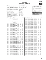
Страница 33: ...emplacer que par une piéce portant le numéro spécifié 1 3 248 142 01 PLATE RETAINER 2 3 246 315 01 SHEET CONTROL 3 A 3178 965 A CONTROL BOARD COMPLETE 4 1 686 493 11 PWB SWITCH FLEXIBLE 5 3 234 449 07 SCREW M1 4 6 3 246 314 01 KNOB OPEN 7 3 246 313 01 COVER CONTROL 8 3 246 312 01 BUTTON CONTROL 9 X 3382 635 1 BRACKET ASSY 10 3 246 203 01 SCREW STEP 11 X 3382 636 1 HOLDER ASSY 12 3 246 318 01 BRACK...

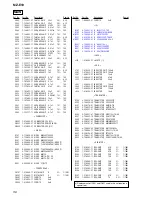
Страница 34: ...56 3 338 645 31 WASHER 0 8 2 5 57 3 244 880 01 SPRING THRUST DETENT 058 X 3383 261 1 OPTICAL PICK UP ASSY ABX 1ES 59 3 244 883 01 GEAR SB 60 A 3174 607 A SCREW BLOCK ASSY LEAD 61 3 244 879 01 SPRING RACK M901 8 835 782 01 MOTOR DC SSM18D SPINDLE M902 8 835 783 01 MOTOR DC SSM21B SLED The components identified by mark 0 or dotted line with mark 0 are critical for safety Replace only with part numbe...

Страница 35: ...0V C508 1 164 939 11 CERAMIC CHIP 0 0022uF 10 50V C509 1 125 777 11 CERAMIC CHIP 0 1uF 10 10V C510 1 117 919 11 TANTAL CHIP 10uF 20 6 3V C511 1 137 762 91 TANTALUM 10uF 20 4V C512 1 164 941 11 CERAMIC CHIP 0 0047uF 10 16V C513 1 164 941 11 CERAMIC CHIP 0 0047uF 10 16V C515 1 107 819 11 CERAMIC CHIP 0 022uF 10 16V C518 1 119 923 81 CERAMIC CHIP 0 047uF 10 10V C519 1 125 837 91 CERAMIC CHIP 1uF 10 6...

Страница 36: ...08A T04 GROUP D851 8 719 077 43 DIODE MAZZ068H01S0 D902 8 719 420 51 DIODE MA729 D903 8 719 071 45 DIODE MA116 TX SO D904 8 719 071 45 DIODE MA116 TX SO D951 6 500 369 01 DIODE FT1J3TP FERRITE BEAD FB101 1 216 864 11 METAL CHIP 0 5 1 10W FB201 1 216 864 11 METAL CHIP 0 5 1 10W FB601 1 414 227 11 FERRITE 0uH FB801 1 414 228 11 FERRITE 0uH FB802 1 414 228 11 FERRITE 0uH FB803 1 469 082 21 FERRITE 0u...

Страница 37: ... RES CHIP 10K 5 1 16W R627 1 218 990 11 SHORT CHIP 0 R628 1 218 969 11 RES CHIP 22K 5 1 16W R801 1 218 989 11 RES CHIP 1M 5 1 16W R802 1 218 989 11 RES CHIP 1M 5 1 16W R803 1 218 941 81 RES CHIP 100 5 1 16W R804 1 218 941 81 RES CHIP 100 5 1 16W R817 1 218 945 11 RES CHIP 220 5 1 16W R818 1 244 161 81 RES CHIP 2 2 5 1 16W R819 1 218 949 11 RES CHIP 470 5 1 16W R901 1 218 985 11 RES CHIP 470K 5 1 1...

Страница 38: ...GE 1 816 921 11 ADAPTOR HEADPHONE PC WM10 3 220 749 01 CASE CARRYING 3 247 809 01 MANUAL INSTRUCTION JAPANESE JEW KR 3 247 809 11 MANUAL INSTRUCTION ENGLISH 3 247 809 21 MANUAL INSTRUCTION FRENCH AEP JEW KR 3 247 809 41 MANUAL INSTRUCTION SPANISH AEP JEW KR 3 247 809 51 MANUAL INSTRUCTION DUTCH AEP 3 247 809 61 MANUAL INSTRUCTION SWEDISH AEP 3 247 809 71 MANUAL INSTRUCTION ITALIAN AEP 3 247 809 81...

Страница 39: ...39 MZ E10 MEMO ...
Страница 40: ...cking the version allows you to jump to the revised page Also clicking the version at the upper right on the revised page allows you to jump to the next revised page Ver Date Description of Revision 1 0 2002 11 New MZ E10 ...

Отзывы: