background image

6

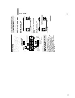
JIG FOR CHECKING BD BOARD WAVEFORM

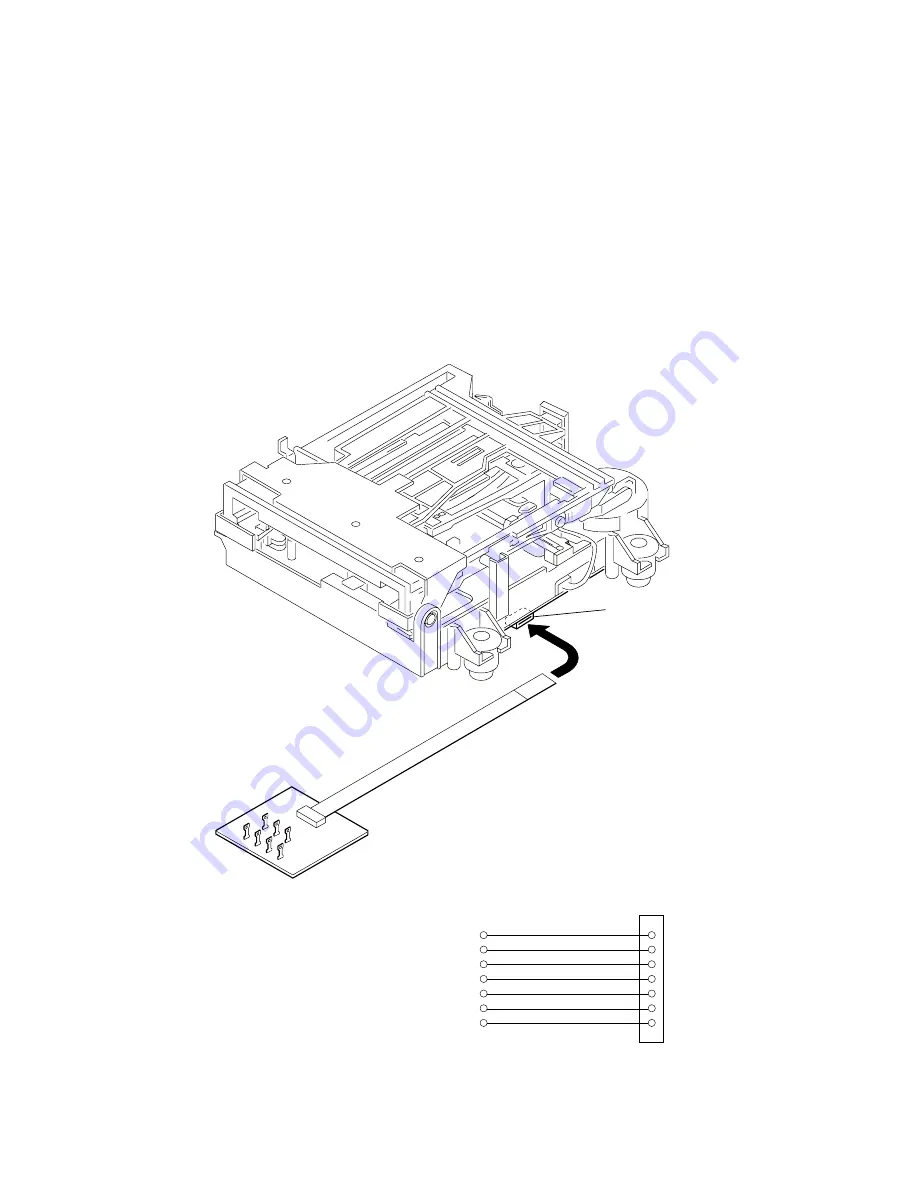
The special jig (J-2501-196-A) is useful for checking the waveform of the BD board. The names of terminals and the checking items to be
performed are shown as follows.

GND : Ground
I+3V : For measuring Iop (Check the deterioration of the optical pick-up laser)
Iop

: For measuring Iop (Check the deterioration of the optical pick-up laser)

TE

: TRK error signal (Traverse adjustment)

VC

: Reference level for checking the signal

RF

: RF signal (Check jitter)

FE

: Focus error signal

I+3V
Iop
GND
TE
FE
VC
RF

I+3V

Iop

GND

TE
FE

VC

RF

1

7

for

MDM-7A

I+3V

CN105

Iop

TE

VC

GND

FE

RF

Содержание MDS-PC3

Страница 1: ...dB during playback Wow and flutter Below measurable limit Inputs LINE ANALOG IN Jack type stereo mini Impedance 47 kilohms Rated input 500 mVrms Minimum input 125 mVrms DIGITAL OPTICAL IN Connector type square optical Impedance 660 nm optical wave length Outputs LINE ANALOG OUT VARIABLE Jack type stereo mini Rated output 1 Vrms at 50 kilohms Load impedance Over 10 kilohms DIGITAL OPTICAL OUT Conne...

Страница 2: ... scratched or substandard in quality Replace the disc and repeat the recording procedure C13 Read Error The deck could not read the TOC on the MD properly Take out the MD and insert it again C14 Toc Error The deck could not read the TOC on the MD properly Insert another disc If possible erase all the tracks on the MD page 29 C41 Cannot Copy The digitally dubbed material cannot be recorded digitall...

Страница 3: ...in hexadecimal from 00 to FF Displays the total number of errors Displays total xx This is displayed in hexadecimal from 00 to FF Displays the past ten errors Displays 0x ErrCd X is the history number The younger the number the more recent is the history 00 is the latest is the error code Select the error history number using the AMS knob Displays the past five retry addresses Displays xx ADRS yyy...

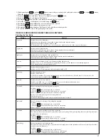
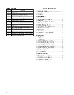
Страница 4: ...tic Diagram Main Section 2 2 43 6 8 Printed Wiring Board Panel Section 44 6 9 Schematic Diagram Panel Section 45 6 10 IC Block Diagrams 46 6 11 IC Pin Functions 49 7 EXPLODED VIEWS 7 1 Chassis Section 54 7 2 Mechanism Section 1 MDM 7A 55 7 3 Mechanism Section 2 MDM 7A 56 8 ELECTRICAL PARTS LIST 57 Table of Error Codes Error Code 10 12 20 21 22 23 24 30 31 40 41 42 43 50 51 Could not load Loading s...

Страница 5: ...T LES NUMÉROS SONT DONNÉS DANS CE MANUEL OU DANS LES SUPPÉMENTS PUBLIÉS PAR SONY This caution label is located inside the unit Lead free soldering MAIN and PANEL boards of this product are lead free soldered contains no lead Lead free solder have the following characteristics The melting point is about 40 ºC higher than conventional solder Conventional soldering iron can be used but must be presse...

Страница 6: ...ollows GND Ground I 3V For measuring Iop Check the deterioration of the optical pick up laser Iop For measuring Iop Check the deterioration of the optical pick up laser TE TRK error signal Traverse adjustment VC Reference level for checking the signal RF RF signal Check jitter FE Focus error signal I 3V Iop GND TE FE VC RF I 3V Iop GND TE FE VC RF 1 7 for MDM 7A I 3V CN105 Iop TE VC GND FE RF ...
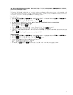
Страница 7: ...nput the Iop value written on the optical pick up To select the number Rotate the AMS knob To select the digit Press the AMS knob 6 When the 1 button is pressed the display becomes Measu is an arbitrary number 7 As the adjustment results are recorded for the 6 value Leave it as it is and press the 1 button 8 Complete will be displayed momentarily The value will be recorded in the non volatile memo...

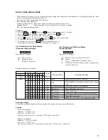
Страница 8: ...e 28 Note The criteria for determination above is intended merely to determine if satisfactory or not and does not serve as the specified value for adjustments When performing adjustments use the specified values for adjustments FORCED RESET The system microprocessor can be reset in the following procedure Use these procedure when the unit cannot be operated normally due to the overrunning of the ...

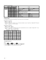
Страница 9: ... Bits Lower Bits 8 4 2 1 8 4 2 1 b7 b6 b5 b4 b3 b2 b1 b0 0 0 0 0 0 0 0 1 0 0 0 0 0 0 1 0 0 0 0 0 0 1 0 0 0 0 0 0 1 0 0 0 0 0 0 1 0 0 0 0 0 0 1 0 0 0 0 0 0 1 0 0 0 0 0 0 1 0 0 0 0 0 0 0 When track jump shock is detected When ADER was counted more than five times continu ously When ADIP address is not continuous When DIN unlock is detected When not in focus When ABCD signal level exceeds the specifi...

Страница 10: ...is case as b2 and b7 are 1 and others are 0 it can be determined that the retry cause is combined of Emphasis OFF Monaural original Copyright exists and Write allowed Example When 07 is displayed Higher bit 0 0000 t All 0 Lower bit 7 0111 t b0 b1 b2 In this case as b0 b1 and b2 are 1 and others are 0 it can be determined that the retry cause is combined of Emphasis ON Stereo Original Copyright exi...

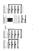
Страница 11: ...ss the switch again the deck turns off and the indicator lights up red 2 PLAY MODE button 24 25 Press to select Shuffle Play or Program Play 3 DISPLAY button 6 16 25 35 Press to select the information to be displayed in the window or to select the type of characters to be input 4 MUSIC SYNC button 20 Press to start Music Synchro recording 5 FADER button 42 Press to perform Fade in Recording Playba...

Страница 12: ...ars only when PGM appears Total number of tracks Total recorded time Total number of tracks and total recorded time default display Press Remaining recordable time on the MD recordable MDs only Press Press Press Order of the programmed tracks The number and total playing time of the programmed tracks Disc name Press R 7 Location and Function of Parts While the deck is recording Press DISPLAY repea...

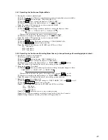
Страница 13: ... editing operations on the PC screen For more details refer to the manual supplied with the PC connecting kit CD player or digital CS tuner etc with optical digital connection capability For PC connecting kit PCLK MN10 Portable CD player etc Active speakers etc Amplifier etc with optical digital connection capability For AC power adaptor Connecting the MD deck with an audio component The MD deck i...

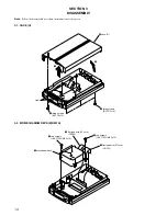
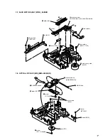
Страница 14: ...te Follow the disassembly procedure in the numerical order given 1 three screws BVTP 3x10 2 3 4 case U 1 three screws BVTP 3x10 claws 2 two screws BVTTWH M3 3x10 3 mechanism deck 2 two screws BVTTWH M3 3x10 1 flat type wire 23 core CN102 1 flat type wire 27 core CN101 ...

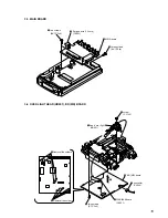
Страница 15: ...RD 1 flat type wire 13 core CN103 2 two screws BVTP 3x8 3 three screws BVTP 3x8 4 MAIN board 6 3 head over light HR901 1 connector CN104 7 FLEXIBLE board CN101 8 BD MD board 2 screw P 1 7x6 5 two screws BTP 2x6 4 Removal the solders 4 Removal the solders ...

Страница 16: ...16 3 5 HOLDER ASSY 3 6 LOADING MOTOR ASSY M103 2 claw 3 5 1 spring holder tension 6 holder assy 4 boss 4 boss 1 belt loading 2 two screws PWH 1 7x2 5 3 motor assy loading M103 ...

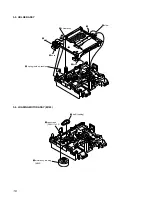
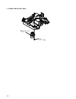
Страница 17: ... screws PWH 1 7x2 5 Remeve the claw Shift the slider in the arrow A direction 2 screw M 1 7 tapping 3 gear SD 6 two screws K 2x6 7 MAIN shaft 8 4 screw BTP 2x6 9 screw P 1 7x6 0 slider SL qa optical pick up KMS 260B J1N 5 base BU A 1 FLEXBLE boaed 3 7 SLED MOTOR ASSY M102 SLIDER 3 8 OPTICAL PICK UP MD KMS 260B JIN ...

Страница 18: ...18 1 screw M 1 7 tapping 2 motor assy spindle M101 3 9 SPINDLE MOTOR ASSY M101 ...

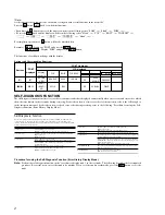
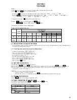
Страница 19: ... Do not use the test mode in the Develop group If used the unit may not operate normally If the Develop group is set accidentally press the x Z button immediately to exit the Develop group 4 3 EXITING THE TEST MODE Press the x Z button remove the power plug to the outlet 4 4 BASIC OPERATIONS OF THE TEST MODE All operations are performed using the AMS knob 1 button and x Z button The functions of t...

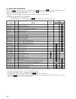
Страница 20: ... version etc Continuous playback mode Continuous recording mode 4 5 SELECTING THE TEST MODE There are 26 types of test modes as shown below The groups can be switched by rotating the AMS knob After selecting the group to be used press the 1 button After setting a certain group rotating the AMS knob switches between these modes Refer to Group in the table for details selected All adjustments and ch...

Страница 21: ...palyback check 1 Entering the continuous recording mode 1 Set a recordable disc in the unit 2 Rotate the AMS knob and display CREC 1MODE C35 3 Press the 1 button to change the display to CREC1 MID 4 When access completes the display changes to CREC1 and REC lights up Note The numbers displayed shows you the recording position addresses 2 Changing the parts to be recorded 1 When the 1 button is pre...

Страница 22: ...ONS OF OTHER BUTTONS 4 7 TEST MODE DISPLAYS Each time the DISPLAY button is pressed the display changes in the following order When CPLAY and CREC are started the display will forcibly be switched to the error rate display as the initial mode 1 Mode display Displays TEMP ADJUST C03 CPLAY1MODE C34 etc 2 Error rate display Displays the error rate in the following way C AD C Indicates the C1 error AD...

Страница 23: ...f a disc is in the mechanical deck it will be ejected forcibly DISC IN will be displayed in this case Load a test disc MDW 74 GA 1 which can be recorded 3 If a disk is loaded at step 2 the check will start automatically 4 When XX CHECK is displayed the item corresponding to XX will be performed When 06 CHECK completes the disc loaded at step 2 will be ejected DISC IN will be displayed Load the che...

Страница 24: ...ick up such as sound skipping are suspected follow the following check Check before replacement Other faults are suspected Check the threading mechanism etc Start NG NG NG OK OK OK Laser Power Check 5 6 2 See page 27 5 6 3 See page 27 5 6 4 See page 28 Iop Compare Auto Check Replace optical pick up or MDM 7A ...

Страница 25: ...ter turning off and then on the power initialize the EEPROM For details refer to 4 11 WHEN MEMORY NG IS DISPLAYED See page 23 Abbreviation OP optical pick up 5 7 INITIAL SETTING OF ADJUSTMENT VALUE See page 30 5 9 TEMPERATURE COMPENSATION OFFSET ADJUSTMENT See page 30 5 10 LASER POWER ADJUSTMENT See page 30 5 12 TRAVERSE ADJUSTMENT See page 31 5 13 FOCUS BIAS ADJUSTMENT See page 32 5 16 AUTO GAIN ...

Страница 26: ...djustments and checks with in the order shown in the following table 2 Set the test mode when performing adjustments After completing the adjustments exit the test mode Perform the adjustments and checks in group S of the test mode 3 Perform the adjustments to be needed in the order shown 4 Use the following tools and measuring devices Check Disc MD TDYS 1 Parts No 4 963 646 01 Test Disk MDW 74 GA...

Страница 27: ...10 Optical pick up label 5 Press the x Z button and display LDPWR CHECK C13 and stop the laser emission The x Z button is effective at all times to stop the laser emission For details of the method for checking this value refer to 5 8 Recording and Displaying Iop Information Note 1 After step 4 each time the 1 button is pressed the display will be switched between LD 0 7 mW LD 6 2 mW and LD Wp Not...

Страница 28: ...y 4 When XX CHECK is displayed the item corresponding to XX will be performed When 06 CHECK completes the disc loaded at step 2 will be ejected DISC IN will be displayed Load the check disc MD TDYS 1 5 When the disc is loaded the check will automatically be resumed from 07 CHECK 6 After completing to test item 12 check OK or NG will be displayed If all items are OK CHECK ALL OK will be displayed I...

Страница 29: ...2 10 Press the x Z button to stop playback and press the x Z PGM button and remove the disc 330 kΩ Oscilloscope 10pF BD board CN105 pin 4 TE CN105 pin 6 VC 5 6 7 Focus Bias Check Change the focus bias and check the focus tolerance amount Checking Procedure 1 Load a continuously recorded test disc MDW 74 GA 1 Refer to 5 5 Using the Continuously Recorded Disc 2 Rotate the AMS knob and display CPLAY1...

Страница 30: ...eled on the pick up indicates Iop value after adjustment 3 To end press the x Z button to display Iop Read C26 5 9 TEMPERATURE COMPENSATION OFFSET ADJUTMENT Save the temperature data at that time in the non volatile memory as 25 C reference data Note 1 Usually do not perform this adjustment 2 Perform this adjustment in an ambient temperature of 22 C to 28 C Perform it immediately after the power i...

Страница 31: ... OFF spindle S servo ON 5 Rotate the AMS knob so that the waveform of the oscilloscope becomes the specified value When the AMS knob is rotated the of EFB changes and the waveform changes In this adjustment waveform var ies at intervals of approx 2 Adjust the waveform so that the specified value is satisfied as much as possible Read power traverse adjustment Traverse Waveform 6 Press the 1 button ...

Страница 32: ...hat it can be seen more clearly 5 13 FOCUS BIAS ADJUSTMENT Adjusting Procedure 1 Load a test disk MDW 74 GA 1 2 Rotate the AMS knob and display CPLAY1MODE C34 3 Press the 1 button and display CPLAY1 MID 4 Press the x Z button when C AD is dis played 5 Rotate the AMS knob and display FBIAS ADJUST C09 6 Press the 1 button and display a T The first four digits indicate the C error rate the two digits...

Страница 33: ... the 1 button and display b Check that the C error is below 100 and ADER is below 2 8 Press the 1 button and display a Check that the C error is below 100 and ADER is below 2 9 Press the x Z button next press the x Z PGM button and remove the continuously recorded disc Note 1 If the C error and ADER are above other than the speci fied value at points a step 8 in the above or b step 7 in the above ...

Страница 34: ...use the jig for checking the waveform Refer to Servicing Note on page 6 BD BOARD SIDE B D101 IC151 23 1 27 1 1 7 IC101 CN101 CN103 CN102 IC195 IC190 CN105 IC102 NOTE 5 17 ADJUSTING POINTS AND CONNECTING POINTS BD BOARD SIDE A ...

Страница 35: ...scilloscope Voltage variations may be noted due to normal produc tion tolerances Circled numbers refer to waveforms Signal path E PB j REC p PB DIGITAL OUT l REC DIGITAL IN Abbreviation CND Canadian model SP Singapore model MY Malaysia model Caution Pattern face side Parts on the pattern face side seen from the Side B pattern face are indicated Parts face side Parts on the parts face side seen fro...

Страница 36: ... XWE XRAS XCAS OE WE RAS CAS D RAM IC153 DIN1 SYSTEM CONTROLLER IC1 1 2 HF MODULE ADDT DADT BCK LRCK Page 37 Page 37 Page 37 SWDT SCLK Page 37 REFLECT PROTECT LD LOW SDA SCL UNREG 5V 11 LIMIT IN OUT SW S101 LIMIT IN PLAY SW SIGNAL PATH PLAY ANALOG OUT PLAY DIGITAL OUT REC ANALOG IN REC DIGITAL IN S103 OUT SW S104 PLAY SW REC P S105 REC POSITION XBCKI LRCKI S102 REFLECT PROTECT DETECT HIGH REFELECT...

Страница 37: ... VARIABLE CN100 ANALOG IN SIGNAL PATH PLAY ANALOG OUT REC ANALOG IN XIN XOUT X22 10MHz SYSTEM CONTROLLER IC1 2 2 RESET 13 14 12 11 15 16 17 19 3 2 5 3 2 7 1 AOUTL AOUTL 26 25 AOUTR AOUTR 28 27 9 9 10 22 26 16 15 LED DRIVE Q701 LED701 LCD701 LCD MODULE LCD BACK LIGHT LED INV DRIVE Q751 D751 14 8 26 115 37 IIC CLK 6 129 4 4 5 124 123 KEY1 139 KEY2 138 KEY0 141 1 3 1 RESET DIG RST 17 47 7 2 128 19 MU...

Страница 38: ... Q134 C 1 Semiconductor Location Ref No Location D181 D 3 D183 D 3 IC101 A 3 IC102 B 3 IC141 C 1 IC151 C 2 IC153 C 3 IC171 D 2 Semiconductor Location Ref No Location There are a few cases that the part isn t mounted in model is printed on diagram IC181 D 3 IC190 D 1 IC195 D 2 Q121 B 3 Q122 B 3 Q181 D 3 Q182 D 3 ...

Страница 39: ...MDS PC3 39 39 6 3 SCHEMATIC DIAGRAM BD SECTION 1 2 See page 35 for Waveforms See page 46 for IC Block Diagrams See page 49 for IC Pin Functions See page 38 for Printed Wiring Board 40 40 40 PIN FUNCTION ...

Страница 40: ... PC3 40 40 6 4 SCHEMATIC DIAGRAM BD SECTION 2 2 See page 35 for Waveforms See page 46 for IC Block Diagrams See page 50 for IC Pin Functions See page 38 for Printed Wiring Board 39 39 39 42 42 PIN FUNCTION ...

Страница 41: ...C 1 Semiconductor Location Ref No Location There are a few cases that the part isn t mounted in model is printed on diagram IC440 B 1 IC451 A 4 IC500 C 5 IC501 B 5 IC502 B 4 IC503 C 5 IC550 D 5 IC600 A 3 IC800 A 2 Q100 B 1 Q170 B 5 Q270 B 5 Q400 B 3 Q440 C 1 Q451 C 5 Ref No Location IC450 A 3 IC611 A 3 IC661 A 4 Q450 D 2 Semiconductor Location MAIN and PANEL boards are lead free soldered contains ...

Страница 42: ...MDS PC3 42 42 6 6 SCHEMATIC DIAGRAM MAIN SECTION 1 2 See page 35 for Waveforms See page 41 for Printed Wiring Board See page 48 for IC Block Diagrams See page 53 for IC Pin Functions PIN FUNCTON ...

Страница 43: ...MDS PC3 43 43 6 7 SCHEMATIC DIAGRAM MAIN SECTION 2 2 See page 35 for Waveforms See page 41 for Printed Wiring Board See page 47 for IC Block Diagrams ...

Страница 44: ...here are a few cases that the part isn t mounted in model is printed on diagram Ref No Location D751 A 6 Q701 A 6 Q751 A 6 Semiconductor Location Ref No Location IC781 A 6 Semiconductor Location MAIN and PANEL boards are lead free soldered contains no lead ...

Страница 45: ...MDS PC3 45 45 6 9 SCHEMATIC DIAGRAM PANEL SECTION See page 35 for Waveforms ...

Страница 46: ... 56 BIAS 55 AVDD 54 ASYI 53 ASYO 52 MVCI 51 D3 68 VC 67 AUX1 66 FE 65 ABCD 64 BOTM 63 PEAK 50 D2 49 D0 48 D1 47 XWE 46 XRAS 45 A09 44 XCAS 43 XOE 42 DVSS 41 A11 40 A08 39 A07 38 A06 37 A05 36 A04 35 A10 34 A00 33 A01 32 A02 31 A03 30 DVDD 28 XBCK 29 FS256 26 DADT 27 LRCK 24 XBCKI 25 ADDT 23 LRCKI 22 DATAI 21 DOUT 20 DIN1 19 DIN0 18 XTSL 17 OSCO 16 OSCI 15 TX 14 XINT 13 RECP 12 DQSY 11 SQSY 10 XRST...

Страница 47: ...27 PD 19 M S 20 CS 17 CCLK 16 CONTROL REGISTER INTERFACE H P F D ATT D ATT S MUTE IC440 LB1830M S TE L MAIN BOARD IC451 XC6351A120MR MAIN BOARD IC500 AK4524 MAIN BOARD 3 GND 2 4 CCE VOUT 5 VIN 6 C1 C1 1 CHIP ENABLE OSCILLATOR P1 BUFFER N2 N3 N4 Q Q Q R S TRIG TRIG MINIMUM ON TIME ONE SHOT MINIMUM OFF TIME ONE SHOT REF ERROR COMPARATOR 1 5V CURRENT SENSE COMPARATOR OUT 3 5 SHDN REF V CS EXT GND 1 2...

Страница 48: ...5TD 118 MAIN BOARD 3 4 5 6 2 8 7 1 VCC NC NC NC RESET GND CD INT INTERRUPT SIGNAL GENERATOR RESET SIGNAL GENERATOR COM R1 R2 R3 R4 COM 5 8 7 BIAS MUTE 0dB VCC LOUT BIAS LIN 3 4 1 2 ROUT MUTE RIN VEE 0dB 180k 180k 6 GND NC NC VCC LCL SCL SDA LDA BUFFER BUFFER 1 5 2 8 7 6 3 4 ...

Страница 49: ...requency setting pin for the internal circuit BPF22 Tracking error signal output to the CXD2662R External capacitor connection pin for the sled error signal LPF Sled error signal output to the CXD2662R FM signal output of ADIP ADIP signal comparator input ADFM is connected with AC coupling External capacitor connection pin for AGC of ADIP ADIP duplex signal output to the CXD2662R I3 signal tempera...

Страница 50: ... L Reset Subcode Q sync SCOR output to the system control L is output every 13 3 msec Almost all H is output Digital In U bit CD format or MD format subcode Q sync SCOR output to the system control Laser power switching input from the system control H Recording L Playback Interrupt status output to the system control Recording data output enable input from the system control System clock input 512...

Страница 51: ...ge 1 5V input from the CXA2523AR Monitor output of the A D converter input signal Not used 3V power supply Analog A D converter operational range upper limit voltage input Fixed at H A D converter operational range lower limit voltage input Fixed at L Ground Analog Sled error signal input from the CXA2523AR Tracking error signal input from the CXA2523AR Connected to 3V power supply Error signal in...

Страница 52: ... I Detection input from the limit switch L Sled limit In H Sled limit Out 31 A1 OUT O Not used 32 XINIT I Interrupt status input from CXD2662R 33 BEEP O Not used 34 LRCK1 O Not used 35 WR PWR O Write power ON OFF output L OFF H ON 36 IIC CLK O IIC clock output 37 IIC DATA I O IIC data input output to the CONTROL I 38 SWDT O Writing data signal output to the serial bus 39 VCC Power supply 3 3V 40 S...

Страница 53: ...er supply 3 3V 92 A8 O Address bus signal output to Flash ROM 93 VSS Ground 94 to 100 A7 to A1 O Address bus signal output to Flash ROM 101 A0 LB O Not used 102 to 113 D15 to D4 I O Data bus signal input output to the Flash ROM 114 KB CLK CTL O Not used 115 IIC BUSY I IIC busy signal input 116 KB DATA I fixed at H Pull up 117 REC VOL B O Not used 118 REC VOL A O Not used 119 to 122 D3 to D0 I O Da...

Страница 54: ...AINBOARD COMPLETE MY SP 22 4 230 476 11 PANEL BACK 23 7 682 248 04 SCREW K 3X8 LCD701 1 804 188 11 LCD MODULE SECTION 7 EXPLODED VIEWS NOTE XX X mean standardized parts so they may have some differences from the original one Items marked are not stocked since they are seldom required for routine service Some delay should be anticipated when ordering these items The mechanical parts with no referen...

Страница 55: ...65 1 SPRING SHT ASSY LEAF 309 4 228 923 01 LOCK HOLDER 310 4 229 533 02 SPRING STOPPER TORSION 311 4 231 118 01 SPRING HOLDER TENSION 312 4 227 019 02 PLATE HOLDER RETAINER 313 4 227 013 01 SPRING EJ TENSION 314 4 226 995 01 SLIDER EJ 315 4 226 996 01 LIMITTER EJ 316 4 226 997 04 SLIDER 317 4 226 998 01 LEVER CHG 318 4 227 006 01 GEAR SA 319 A 4735 075 A HOLDER ASSY 320 4 226 994 01 GUIDE L 321 7 ...

Страница 56: ...6 265 01 SHAFT MAIN 361 4 226 989 01 CHASSIS 362 4 211 036 01 SCREW 1 7X2 5 PWH 363 4 226 990 01 BASE BU A 364 4 227 023 01 SPRING SPINDLE TORSION 365 4 227 004 01 GEAR LC 366 4 227 005 01 GEAR LD 367 4 227 009 01 GEAR SD 368 4 227 008 01 GEAR SC 369 7 685 204 19 SCREW KTP 2X6 TYPE2 NON SLIT M101 A 4672 898 A MOTOR ASSY SPINDLE M102 A 4672 900 A MOTOR ASSY SLED M103 A 4672 975 A MOTOR ASSY LOADING...

Страница 57: ...RAMIC CHIP 0 0047uF 10 50V C166 1 125 891 11 CERAMIC CHIP 0 47uF 10 10V C167 1 164 245 11 CERAMIC CHIP 0 015uF 10 25V C169 1 164 156 11 CERAMIC CHIP 0 1uF 25V C171 1 164 156 11 CERAMIC CHIP 0 1uF 25V C172 1 164 156 11 CERAMIC CHIP 0 1uF 25V C180 1 117 370 11 CERAMIC CHIP 10uF 10V C181 1 126 206 11 ELECT CHIP 100uF 20 6 3V C182 1 163 038 11 CERAMIC CHIP 0 1uF 25V C183 1 164 156 11 CERAMIC CHIP 0 1u...

Страница 58: ...15 1 216 833 11 METAL CHIP 10K 5 1 16W R116 1 216 839 11 METAL CHIP 33K 5 1 16W R117 1 216 837 11 METAL CHIP 22K 5 1 16W R118 1 218 855 11 METAL CHIP 2 2K 0 5 1 16W R119 1 218 863 11 METAL CHIP 4 7K 0 5 1 16W R120 1 218 889 11 METAL CHIP 56K 0 5 1 16W R121 1 218 863 11 METAL CHIP 4 7K 0 5 1 16W R122 1 218 855 11 METAL CHIP 2 2K 0 5 1 16W R123 1 216 819 11 METAL CHIP 680 5 1 16W R124 1 216 809 11 M...

Страница 59: ...P 0 1uF 25V C321 1 801 862 11 VARISTOR CHIP 1050PF 7 5V C401 1 164 156 11 CERAMIC CHIP 0 1uF 25V C402 1 164 156 11 CERAMIC CHIP 0 1uF 25V C404 1 164 156 11 CERAMIC CHIP 0 1uF 25V C406 1 164 156 11 CERAMIC CHIP 0 1uF 25V C407 1 128 547 11 ELECT 6800uF 20 16V C408 1 164 156 11 CERAMIC CHIP 0 1uF 25V C409 1 164 156 11 CERAMIC CHIP 0 1uF 25V C410 1 119 879 11 ELECT 15uF 16V C412 1 119 765 11 ELECT 47u...

Страница 60: ...4 11 CONNECTOR DIN 6P PC LINK COIL L151 1 216 864 11 METAL CHIP 0 5 1 16W L178 1 414 760 21 FERRITE 0uH L180 1 414 760 21 FERRITE 0uH L251 1 216 864 11 METAL CHIP 0 5 1 16W L278 1 414 760 21 FERRITE 0uH L280 1 414 760 21 FERRITE 0uH L400 1 424 674 11 INDUCTOR 22uH L501 1 414 760 21 FERRITE 0uH L502 1 414 760 21 FERRITE 0uH L503 1 414 760 21 FERRITE 0uH L504 1 216 864 11 METAL CHIP 0 5 1 16W L550 1...

Страница 61: ...ETAL CHIP 220 5 1 16W R502 1 216 813 11 METAL CHIP 220 5 1 16W R503 1 216 813 11 METAL CHIP 220 5 1 16W R504 1 216 809 11 METAL CHIP 100 5 1 16W R505 1 216 809 11 METAL CHIP 100 5 1 16W R506 1 216 809 11 METAL CHIP 100 5 1 16W R550 1 216 857 11 METAL CHIP 1M 5 1 16W R551 1 414 760 21 FERRITE 0UH R552 1 216 813 11 METAL CHIP 220 5 1 16W R554 1 216 815 11 METAL CHIP 330 5 1 16W R600 1 216 853 11 MET...

Страница 62: ...541 A OPTICAL PICK UP KMS 260B J1N M101 A 4672 898 A MOTOR ASSY SPINDLE M102 A 4672 900 A MOTOR ASSY SLED M103 A 4672 975 A MOTOR ASSY LOADING S102 1 771 957 11 SWITCH PUSH 2 KEY REFLECT PROTECT SW HR901 1 500 670 12 HEAD OVER LIGHT LCD701 1 804 188 11 LCD MODULE LED701 1 804 189 11 LIGHT LCD BACK ACCESSORIES PACKING MATERIALS A 4680 613 A OVERALL ASSY PCLK MN10 1 469 089 11 FILTER CLAMP FERRITE C...

Отзывы: