MDR-RF845R
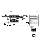
4-1. BLOCK DIAGRAM
— 7 —
— 8 —
L301
RECEIVE
FREQ.
D301
+V
+V
FRONT END
FE UNIT
18
13
16
FM IF/
DISCRI
DECODE
AMP
DETUNE
MUTE
TUNING
IND
STEREO
IND
CF301
26
CF302
10.7MHz
6
2
10
9
5
R-CH
R-CH
RV302
VOLUME
SPEAKER
L-CH
SPEAKER
R-CH
POWER AMP
IC302
MUTE
Q304
22
20
FM FE
L302
+V
D/A
CONV
IC303
DETECT
IC304
FF
IC303
OSC
Q301
SWITCH
Q303
10
12
27
S301
TUNING
Q305
D
Q
Q
AUTO
BLEND
MUTE
MONO/ST
SW
1/2
COUNTER
PD1
PD1
VCO
21
REG
RV301
FREE RUN
FREQ.
IF AMP/DECODE
IC301
D304
S1
ON/OFF SW
+
-
B+
• Signal path.
: FM
16
POWER
SECTION 4
DIAGRAMS
•
IC BLOCK DIAGRAMS
IC302 LA4533M
IC303 TC7W74FU
POWER
SWITCH
MUTE
CIRCIUT
BIAS
1
2
3
4
5
6
7
8
9
10 MT/SW
OUT1
POWER GND
OUT2
VCC
P/SW
IN1
PRE GND
IN2
REF
AMP2
AMP1
6
CLR
7
PR
8
VCC
5
Q
R
S
Q
3
Q
2
D
4
GND
1
CK
Q
D
C
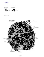
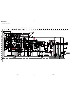
Note on Schematic Diagram:
• All capacitors are in µF unless otherwise noted. pF: µµF 50 WV or
less are not indicated except for electrolytics and tantalums.
• All resistors are in
Ω
and
1
/
4
W or less unless otherwise specified.
•
¢
: internal component.
•
A
: B+ Line.
•
H
: adjustment for repair.
• Power voltage is dc 2.4 V and fed with regulated dc power supply
from battery terminal.
• Voltages are dc with respect to ground under no-signal conditions.
• Voltages are taken with a VOM (Input impedance 10 M
Ω
).
Voltage variations may be noted due to normal production toler-
ances.
• Waveforms are taken with a oscilloscope.
Voltage variations may be noted due to normal production toler-
ances.
• Circled numbers refer to waveforms.
• Signal path.
F
:
FM
L
: AUDIO
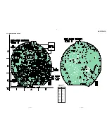
Note on Printed Wiring Board:
•
X
: parts extracted from the component side.
•
®
: Through hole.
•
b
: Pattern from the side which enables seeing.
Caution:
Pattern face side:
Parts on the pattern face side seen from
(SideB)
the pattern face are indicated.
Parts face side:
Parts on the parts face side seen from
(Side A)
the parts face are indicated.
Содержание MDR-RF845R
Страница 8: ...MDR RF845R 4 2 SCHEMATIC DIAGRAM 9 10 ...
Страница 10: ...MDR RF845R MEMO ...


