


TMR-RF815R
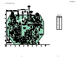
4-1. BLOCK DIAGRAM
— 5 —
— 6 —
SECTION 4
DIAGRAMS
J401
S401
NOISE FILTER
NOISE
FILTER
INPUT
AMP
CH1
AMP
BUFFER
BUFFER
Q401
RECT
D404,405
2V
D408
INPUT
DET
DIVIDER
BUFFER
OSC
AMP
TIME
DEVISION
MPX
AUDIO IN
B
J402
A
OFF
|
ON
S402
CHANNEL
L
R
R-CH
R-CH
R-CH
1
9
8
13
10
12
11
6
7
9
15
7
6
CH2
AMP
14
X401
38kHz
RV403
MOD IN
CE DI CL
CE DI CL
VS
16
5V
VCO CONTROLLER
IC404
IC401
LPF
IC403
STEREO MPX
IC405(1/2)
IC405(2/2)
+5V
REG
SWITCH
Q404
+4V
Q402
POWER OFF
DET
IC402
ANT
5V
B+
T-OUT
ANT401
D401
D402
J404
DC IN 9V
CHARGE
POWER
CHG
1
2
3
VCO UNIT
• Signal path.
: AUDIO
16
Note on Printed Wiring Board:
•
X
: parts extracted from the component side.
•
b
: Pattern from the side which enables seeing.
Note on Schematic Diagram:
• All capacitors are in µF unless otherwise noted. pF: µµF 50 WV or
less are not indicated except for electrolytics and tantalums.
• All resistors are in
Ω
and
1
/
4
W or less unless otherwise specified.
•
f
: internal component.
•
A
: B+ Line.
•
H
: adjustment for repair.
• Power voltage is dc 9 V and fed with regulated dc power supply
from battery terminal.
• Voltages are dc with respect to ground under no-signal conditions.
• Voltages are taken with a VOM (Input impedance 10 M
Ω
).
Voltage variations may be noted due to normal production toler-
ances.
• Waveforms are taken with a oscilloscope.
Voltage variations may be noted due to normal production toler-
ances.
• Circled numbers refer to waveforms.
• Signal path.
L
: AUDIO