34
MCE-SV7
•
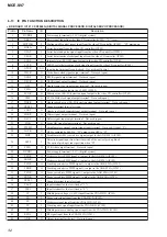
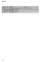
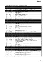
VMP BOARD IC502 M30622MGA-A59FP (VIDEO CD CONTROLLER)
Pin No.
Pin Name
I/O
Description
1
SENSE
I
Internal status (SENSE) signal input from the CXD3068Q (IC101)
2
SENSE CLK
O
Sense serial data reading clock signal output to the CXD3068Q (IC101)
3
RESOLUTION
O
Serial data output to the Y amplifier (IC303)
4
CROMA LEVEL
O
Serial data latch pulse output to the C amplifier (IC302)
5
DSP CLK
O
Serial data transfer clock signal output to the CXD3068Q (IC101)
6
TSENS
I
Disc tray status detection signal input terminal Not used (open)
7
REMOTE IN
I
Remote control signal input terminal Not used (open)
8
BYTE
I
External data bus line byte selection signal input terminal
“L”: 16 bit, “H”: 8 bit (fixed at “L”)
9
CNVSS
—
Ground terminal Not used
10
DSP MUTING
O
Muting on/off control signal output to the CXD3068Q (IC101) “H”: muting on
11
CTRL1
O
Clock selection signal output to the CXD3068Q (IC101)
“L”: 16.9344 MHz (double speed), “H”: 33.8688 MHz
12
XRESET
I
Reset signal input from the tuner unit (ST-SV7) “L”: reset
13
XOUT
O
Main system clock output terminal (10 MHz)
14
VSS
—
Ground terminal
15
XIN
I
Main system clock input terminal (10 MHz)
16
VCC
—
Power supply terminal (+5V)
17
NMI
I
Non-maskable interrupt input terminal (fixed at “H” in this set)
18
SCOR
I
Subcode sync (S0+S1) detection signal input from the CXD3068Q (IC101)
19
DSENS
I
Disc status detection signal input terminal Not used (open)
20
CL680 HINT
I
Interrupt request signal input from the CL680T (IC505)
21
H.SYNC IN
O
Horizontal synchronized signal input from the CL680T (IC505)
22
BGP
O
BGP signal output to the C amplifier (IC302)
23
—
—
Not used (open)
24
PWM3
O
RFDC PWM signal output to the CXA2581N (IC103)
25
—
—
Not used (open)
26
PWM2
O
PWM signal output to the CXA2581N (IC103)
27
—
—
Not used (open)
28
PWM1
O
Focus servo drive PWM signal output to the CXA2581N (IC103)
29
I2C.CLK
I/O
Communication data reading clock signal input or transfer clock signal output with the system
controller (IC401) and tuner unit (ST-SV7)
30
I2C.DATA
I/O
Communication data bus with the system controller (IC401) and tuner unit (ST-SV7)
31
DATA1O
O
Serial data output terminal Not used
32
DATA1I
I
Serial data input terminal Not used
33
CLK1
O
Serial data transfer clock signal output terminal Not used
34
RTSI
I
Reset signal input terminal Not used
35
DATAO
O
Serial data output to the CL680T (IC505) and D/A converter (IC509)
36
DATAI
I
Serial data input from the CL680T (IC505)
37
CLKI
O
Serial data transfer clock signal output to the CL680T (IC505) and D/A converter (IC509)
38
P.ON
O
Power on/off control signal output terminal Not used (open)
39
BUS XRDY
I
Ready signal input terminal Not used (fixed at “H”)
40
BUS
O
Not used (open)
41
BUS XHOLD
I
Hold signal input terminal Not used (fixed at “H”)
42, 43
BUS
O
Not used (open)
44
OSD.LANGUAGE
I
Destination setting terminal “L”: chinese, “H”: others (fixed at “H” in this set)
45
VSYNC
I
Vertical synchronized signal input from theCL680T (IC505) “L” active
Содержание MCE-SV7
Страница 53: ...53 MCE SV7 MEMO ...


