37
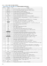
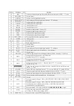
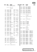
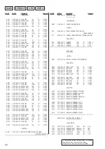
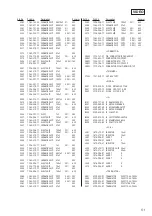
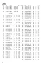
(MPEG VIDEO/AUDIO DECODER, VIDEO SIGNAL PROCESSOR)
Pin No.
Pin Name
I/O
Function
1
NC
O
Not used (open)
2
VSS
—
Ground terminal
3
CD-BCK
I
CD decode bit clock signal (2.8224 MHz) input from the CXD2545Q (IC101)
4
CD-DATA
I
CD decode data input from the CXD2545Q (IC101)
5
CD-LRCK
I
CD decode L/R sampling clock signal (44.1 kHz) input from the CXD2545Q (IC101)
6
CD-C2PO
I
CD decode C2 error data input from the CXD2545Q (IC101)
7 to 9
NC
O
Not used (open)
10 to 15
MD0 to MD5
I/O
Two-way data bus with the program ROM (IC506) and D-RAM (IC507)
16
VSS
—
Ground terminal
17
MD6
I/O
Two-way data bus with the program ROM (IC506) and D-RAM (IC507)
18
VDD3
—
Power supply terminal (+3.3V)
19
MD7
I/O
Two-way data bus with the program ROM (IC506) and D-RAM (IC507)
20
VSS
—
Ground terminal
21
MD8
I/O
Two-way data bus with the program ROM (IC506) and D-RAM (IC507)
22
VDD3
—
Power supply terminal (+3.3V)
23 to 28
MD9 to MD14
I/O
Two-way data bus with the program ROM (IC506) and D-RAM (IC507)
29
MD15
I/O
Two-way data bus with the D-RAM (IC507)
30 to 36
NC
O
Not used (open)
37
MCE
O
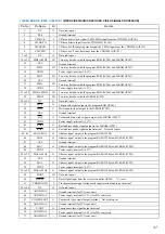
Chip enable signal output to the program ROM (IC506)
38
MWE
O
Write enable signal output to the D-RAM (IC507)
39
VSS
—
Ground terminal
40
CAS
O
Column address strobe signal output to the D-RAM (IC507)
41
VDD3
—
Power supply terminal (+3.3V)
42
RAS0
O
Row address strobe signal output to the D-RAM (IC507)
43
RAS1
O
Row address strobe signal output terminal Not used (open)
44, 45
MA10, MA9
O
Address signal output to the program ROM (IC506)
46
MA8
O
Address signal output to the program ROM (IC506) and D-RAM (IC507)
47
VSS
—
Ground terminal
48
MA7
O
Address signal output to the program ROM (IC506) and D-RAM (IC507)
49
VDD3
—
Power supply terminal (+3.3V)
50 to 52
MA6 to MA4
O
Address signal output to the program ROM (IC506) and D-RAM (IC507)
53
VSS
—
Ground terminal
54
MA3
O
Address signal output to the program ROM (IC506) and D-RAM (IC507)
55
VDD3
—
Power supply terminal (+3.3V)
56 to 58
MA2 to MA0
O
Address signal output to the program ROM (IC506) and D-RAM (IC507)
59
PGIO7
I/O
Not used (open)
60
RESET
I
Reset signal input from the system controller (IC502) “L”: reset
61
VDDMAX-IN
I
Fix the maximum input voltage each input terminal and in/out terminal
62 to 64
NC
O
Not used (open)
65
AGND-DAC
—
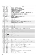
Ground terminal (for D/A converter)
66
AVDD-DAC
—
Power supply terminal (+3.3V) (for D/A converter)
67
COMPOS OUT
O
Composite video signal output terminal Not used (open)
68
AGND-DAC
—
Ground terminal (for D/A converter)
69
Y-OUT
O
Luminance video signal output terminal
70
AVDD-DAC
—
Power supply terminal (+3.3V) (for D/A converter)
71
AGND-DAC
—
Ground terminal (for D/A converter)

